SE SEM IV Syllabus
| se3-4-etrx-2013.pdf |
| instructions_to_write_dec_journal.pdf |
In this video differential amplifier basics is discussed.
In the video shown during lecture dated 5-4-2017, focus only on LOWER CUTOFF frequency for now.
Syllabus for DEC 2017 Mid term 2
1. DC Analysis of JFET and MOSFET: Weightage : 03 -05 M
a) For JFET : Fixed bias , self bias , midpoint bias and voltage divider bias circuits.
b) For MOSFET : 1. D-type MOSFET biasing( self bias, voltage divider bias, etc..)
2. E-type MOSFET biasing (Zero drain feedback, Voltage divider biasing , etc ...)
i) Derivation for Q point for above biasing circuits
ii) Numericals (analytical & graphical) and design of above biasing circuits
NOTE : Draw DC load line on graph paper if asked in exam
2. JFET and MOSFET as single stage amplifers ( CS, CG and CD) Weightage: 05 - 07 M
a) Analysis of CS amplifier ( JFET & MOSFET )
i ) Derivation of Zi , Zo and Av
ii) Effect of adding load RL or source resistance Rs on gain Av
iii) Numericals
b) Analysis of CS stage ( JFET & MOSFET ) with source degeneration
i ) Derivation of Zi , Zo and Av
ii) Effect of adding load RL or source resistance Rs on gain Av
iii) Numericals
iv) Features of source degeneration CS stage
c) Analysis of CD ( JFET & MOSFET ) amplifier
i ) Derivation of Zi , Zo and Av
ii) Effect of adding load RL or source resistance Rs on gain Av
iii) Numericals
d) Analysis of CG ( JFET & MOSFET ) amplifier
i ) Derivation of Zi , Zo and Av
ii) Effect of adding load RL or source resistance Rs on gain Av
iii) Numericals
Attention: JFET ac analysis and MOSFET ac analysis are identical [ All derivations are similar, only symbolwise (JFET n MOSFET ) they differ]
3. Multi stage amplifiers Weightage: 05 - 07 M
Need of Cascading of amplifiers
a) Analysis of CE-CE amplifier
i ) Derivation of Zi , Zo and Av
ii) Effect of adding load RL or source resistance Rs on gain Av
iii) Numericals
b) Analysis of CS-CS amplifier ( JFET or MOSFET )
i ) Derivation of Zi , Zo and Av
ii) Effect of adding load RL or source resistance Rs on gain Av
iii) Numericals
c) Analysis of CS-CE cascade amplifier
i ) Derivation of Zi , Zo and Av
ii) Effect of adding load RL or source resistance Rs on gain Av
iii) Numericals
d) Analysis of CE-CB cascode or CS-CG cascode amplifier
i ) Derivation of Zi , Zo and Av
ii) Effect of adding load RL or source resistance Rs on gain Av
iii) Numericals
e) Darlinton pair
i) Its necessity
ii) Features
iii) Current gain derivation
iv) Applications
4. Negative feedback amplifiers Weightage: 05 M
Types of Negative Feedback, block diagram representation, Effect of negative feedback on Input impedance, Output impedance, Gain and Bandwidth with derivation for different feedback topologies.
NOTE : In all the derivations of Zi , Zo and Av , it is necessary to
1. Draw small signal equivalent circuit for the given circuit.
2. Add these lines to your answer : Assumption : Capacitors in the circuits have zero impedance for Ac signals, hence we replace them by short circuit.
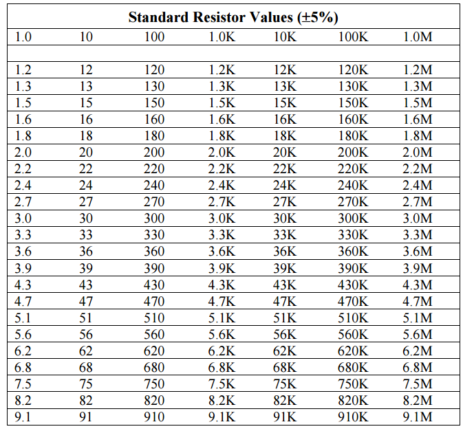
3. Use standard value of resistors in design problems
4. Solve assignment no 2 ( B1 B2 B3 and B4) , before mid term 2
1. DC Analysis of JFET and MOSFET: Weightage : 03 -05 M
a) For JFET : Fixed bias , self bias , midpoint bias and voltage divider bias circuits.
b) For MOSFET : 1. D-type MOSFET biasing( self bias, voltage divider bias, etc..)
2. E-type MOSFET biasing (Zero drain feedback, Voltage divider biasing , etc ...)
i) Derivation for Q point for above biasing circuits
ii) Numericals (analytical & graphical) and design of above biasing circuits
NOTE : Draw DC load line on graph paper if asked in exam
2. JFET and MOSFET as single stage amplifers ( CS, CG and CD) Weightage: 05 - 07 M
a) Analysis of CS amplifier ( JFET & MOSFET )
i ) Derivation of Zi , Zo and Av
ii) Effect of adding load RL or source resistance Rs on gain Av
iii) Numericals
b) Analysis of CS stage ( JFET & MOSFET ) with source degeneration
i ) Derivation of Zi , Zo and Av
ii) Effect of adding load RL or source resistance Rs on gain Av
iii) Numericals
iv) Features of source degeneration CS stage
c) Analysis of CD ( JFET & MOSFET ) amplifier
i ) Derivation of Zi , Zo and Av
ii) Effect of adding load RL or source resistance Rs on gain Av
iii) Numericals
d) Analysis of CG ( JFET & MOSFET ) amplifier
i ) Derivation of Zi , Zo and Av
ii) Effect of adding load RL or source resistance Rs on gain Av
iii) Numericals
Attention: JFET ac analysis and MOSFET ac analysis are identical [ All derivations are similar, only symbolwise (JFET n MOSFET ) they differ]
3. Multi stage amplifiers Weightage: 05 - 07 M
Need of Cascading of amplifiers
a) Analysis of CE-CE amplifier
i ) Derivation of Zi , Zo and Av
ii) Effect of adding load RL or source resistance Rs on gain Av
iii) Numericals
b) Analysis of CS-CS amplifier ( JFET or MOSFET )
i ) Derivation of Zi , Zo and Av
ii) Effect of adding load RL or source resistance Rs on gain Av
iii) Numericals
c) Analysis of CS-CE cascade amplifier
i ) Derivation of Zi , Zo and Av
ii) Effect of adding load RL or source resistance Rs on gain Av
iii) Numericals
d) Analysis of CE-CB cascode or CS-CG cascode amplifier
i ) Derivation of Zi , Zo and Av
ii) Effect of adding load RL or source resistance Rs on gain Av
iii) Numericals
e) Darlinton pair
i) Its necessity
ii) Features
iii) Current gain derivation
iv) Applications
4. Negative feedback amplifiers Weightage: 05 M
Types of Negative Feedback, block diagram representation, Effect of negative feedback on Input impedance, Output impedance, Gain and Bandwidth with derivation for different feedback topologies.
NOTE : In all the derivations of Zi , Zo and Av , it is necessary to
1. Draw small signal equivalent circuit for the given circuit.
2. Add these lines to your answer : Assumption : Capacitors in the circuits have zero impedance for Ac signals, hence we replace them by short circuit.
3. Use standard value of resistors in design problems
4. Solve assignment no 2 ( B1 B2 B3 and B4) , before mid term 2
Assignment no 02
Date of submission : 30th March, 2017
Please submit your Assignment no 1 also on the same day
Note : Assignment 02 is batch wise
Date of submission : 30th March, 2017
Please submit your Assignment no 1 also on the same day
Note : Assignment 02 is batch wise
| dec_assg02_b1.pdf |
| dec_assg02_b2.pdf |
| dec_assg02_b3.pdf |
| dec_assg02_b4.pdf |
Syllabus for DEC 2017 Mid term 1
1. Application of Diodes : a) Analysis of clipper ( 13 ) and clamper circuits ( 06 ) using ideal diode and constant voltage model. Weightage : 05 M
2. DC Analysis of BJT biasing circuits : Weightage : 05 -12M
a) Derivation for Q point for various biasing circuits
b) Numericals and design of various biasing circuits
c) Concept of DC load line
NOTE : Draw DC load line on graph paper if asked in exam
3. BJT as amplifer ( CE, CC and CB stages) Weightage: 10 - 12M
a) Necessity of DC biasing and derivation for r_pi , gm and r_o for hybrid pi model for npn transistor.
b) Concept of input and output impedance
c) Analysis of CE amplifier in detail
i ) Derivation of Zi , Zo and Av
ii) Effect of adding load RL or source resistance Rs on gain Av
iii) Numericals
d) Analysis of CE stage with emitter degeneration in details
i ) Derivation of Zi , Zo and Av
ii) Effect of adding load RL or source resistance Rs on gain Av
iii) Numericals
iv) Features of emitter degeneration CE stage
e) Analysis of CC amplifier in detail
i ) Derivation of Zi , Zo and Av
ii) Effect of adding load RL or source resistance Rs on gain Av
iii) Numericals
d) Analysis of CB amplifier in detail
i ) Derivation of Zi , Zo and Av
ii) Effect of adding load RL or source resistance Rs on gain Av
iii) Numericals
NOTE : In all the derivations of Zi , Zo and Av , it is necessary to
1. Draw small signal equivalent circuit for the given circuit.
2. Add these lines to your answer : Assumption : Capacitors in the circuits have zero impedance for Ac signals, hence we replace them by short circuit.
3. Use standard value of resistors in design problems
4. Solve assignment 1, before mid term 1, it will come in handy.
DEC Assignment No 01
D.O.S : 01/03/2017
D.O.S : 01/03/2017
| dec_assg01.pdf |
LINK : http://www.learnabout-electronics.org/Amplifiers/amplifiers12.php
