"An investment in knowledge pays the best interest"
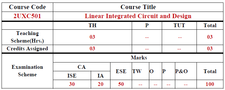
Syllabus (KJSCE 2014)
Reference Books
1. D. Roy Choudhry, Shail Jain, “Linear Integrated Circuits”, Fourth edition, New Age International Pvt. Ltd., 2010.
2. Sergio Franco, “Design with operational amplifiers and analog integrated circuits”, Fourth edition, McGraw Hill International edition, 2014.
3. Ramakant A. Gayakwad, “OP-AMP and Linear IC’s”, Sixth edition, Prentice Hall / Pearson Education, 1999.
4. Anant Agrawal, Jefferey H. Lang, "Foundations of Analog and digital Electronics Circuits", Elsevier, 2005
5. Robert Coughlin and F Driscoll, “Operational Amplifiers and Linear Integrated circuits”, Sixth edition, Pearson Education Asia, 2001.
E-books
| agarwal_and_lang__2005__foundations_of_analog_and_digital.pdf |
Lecture 01 handout dated 17-07-2018
Topics Covered : Op amp Abstraction, Op amp Symbol, Circuit Model of Op amp( Ideal case) , Ideal op amp properties , a look at op amp tranfer characteristics
Topics Covered : Op amp Abstraction, Op amp Symbol, Circuit Model of Op amp( Ideal case) , Ideal op amp properties , a look at op amp tranfer characteristics
| licd_01.pdf |
Videos related to lecture 01 are below : 01.01 to 01.05 ( Total 5 )
Idea behind the making video's lectures available is to make an attempt to involve an environment to learn continuously and at one's pace. It will also help those who have missed lectures and wants to resume the topic. One can really Do that !!!
Use it Wisely !!!!
Video Reference : MITx: 6.002.3x
Video 01.01 : Op amp abstraction
Video 01.02 : Op amp Insight: A look at Op amp Symbol
Video 01.03 : Circuit Model of Ideal Op amp and its properties
Video 01.04 : Op amp Characteristics
Video 01.05 : Op amp Characteristics Demo ( Only for understanding)
This is Fun ... you get to see open loop tranfer characteristics of opamp and reflect on notorious unreliable behavior of Op amps gain...
This is Fun ... you get to see open loop tranfer characteristics of opamp and reflect on notorious unreliable behavior of Op amps gain...
Lecture 02 handout dated 18-07-2018
Topics Covered : 1st Op amp Circuit : Non inverting amplifier ( Analyses) with circuit model, Power of negative feedback and its effect on Opamp Circuit, Real Life example of Negative feedback ( Anti-Lock Brakes System) , Concept of virtual Short, Applying Virtual short concept to Non-inverting amplifier.
Topics Covered : 1st Op amp Circuit : Non inverting amplifier ( Analyses) with circuit model, Power of negative feedback and its effect on Opamp Circuit, Real Life example of Negative feedback ( Anti-Lock Brakes System) , Concept of virtual Short, Applying Virtual short concept to Non-inverting amplifier.
| licd_02.pdf |
Videos related to lecture 02 are below : 02.01 to 02.06 ( Total 6 )
Video 02.01 : Our First Circuit : Non inverting amplifier using Op amp (Part 1)
Remember the analogy to Car: Its like First time experiencing once you get inside the car....
Remember the analogy to Car: Its like First time experiencing once you get inside the car....
Video 02.02 : Non inverting amplifier using Op amp (Part 2)
Video 02.03 : Demo - Op Amp is Stable in Non-Inverting Circuit Configuration
This is Fun ... you get to see closed loop tranfer characteristics of non-inverting opamp
Many of you must have seen it in LICD LABORATORY while performing experiment on Non-invering amplifier using Op amp
Observe HOW STABLE CIRCUIT GAIN is in DEMO .... ITS ROCK SOLID
This is Fun ... you get to see closed loop tranfer characteristics of non-inverting opamp
Many of you must have seen it in LICD LABORATORY while performing experiment on Non-invering amplifier using Op amp
Observe HOW STABLE CIRCUIT GAIN is in DEMO .... ITS ROCK SOLID
Video 02.04 : Antilock Brakes and Negative Feedback ( ONLY FOR understanding)
This video was shown Live in the class
This video was shown Live in the class
Video 02.05 : Virtual Short Method
Video 02.06 : Analysis of Non-inverting Amplifier using Virtual Short Method
Lecture 03 handout dated 19-07-2018
Topics Covered : Analysis of Unity Gain Buffer and its requirement, Inverting amplifier ( Analysis) using circuit model and Virtual short technique, input resistance of Inverting and non-inverting amplifier comparison, Simulation Demo shown of circuits like Inverting, non-inverting and buffer circuit on LT-SPICE.
Topics Covered : Analysis of Unity Gain Buffer and its requirement, Inverting amplifier ( Analysis) using circuit model and Virtual short technique, input resistance of Inverting and non-inverting amplifier comparison, Simulation Demo shown of circuits like Inverting, non-inverting and buffer circuit on LT-SPICE.
| licd_03.pdf |
Videos related to lecture 03 are below : 03.01 to 03.05 ( Total 5 )
Video 03.01 : Unity Gain Buffer Circuit
Video 03.02 : Why is Unity Gain Buffer Circuit useful ?
Video 03.03 : Inverting Amplifier Circuit Analysis using Op amp Circuit Model
Video 03.04 : Inverting Amplifier Circuit Analysis using Virtual Short Technique
Video 03.05 : Inverting Amplifier input resistance estimation using Virtual Short method
Lecture 04 handout dated 20-07-2018
Topics Covered : Inverting adder Analysis and its application, Case of Averaging amplifier, Implementation of Linear equation using Inverting adder and its Simulation Demo shown, Exposure to LT Spice by implementing inverting amplifier circuit from scratch LIVE in class, Non-inverting adder topic given to students as Self study
Topics Covered : Inverting adder Analysis and its application, Case of Averaging amplifier, Implementation of Linear equation using Inverting adder and its Simulation Demo shown, Exposure to LT Spice by implementing inverting amplifier circuit from scratch LIVE in class, Non-inverting adder topic given to students as Self study
| licd_04.pdf |
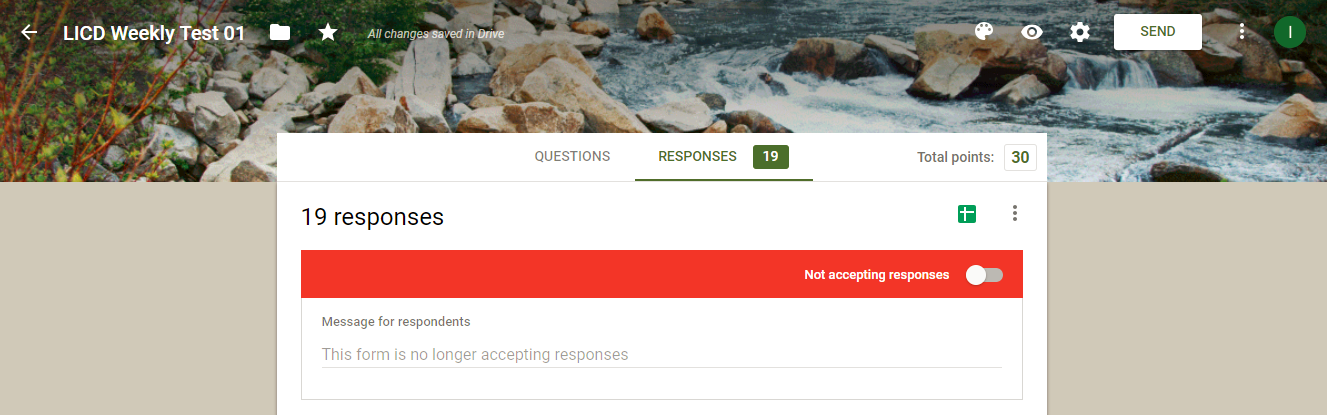
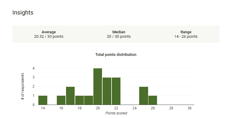
LICD Weekly Test 01 : coming soon by 11am on 21/7/2018 on Google Classroom and in this website:
Join Google Classroom via your Somaiya email ids
Steps :
1. Open Google Classroom
2. Join Class
3. Class Code is 3dfgyx1
Announcement:
Test is active now, an email link has been send
Test will remain active till 23:59 Hrs 22/7/2018
Those who haven't received the email can access Test via the link given below:
https://docs.google.com/forms/d/e/1FAIpQLSfLr-Ha3hcW60E_kf0GKsmsepZLZJWzDwAHJLEQLbBYIM4Ycg/viewform?usp=sf_link
End of Week 01: 17-07-2018 to 20-07-2018
Total no. of Lectures conducted: 04
Total Hours: 04
Activities during week 01:
1) Exposure to LTSpice schematic and simulation tool
2) Use of LIVE Quiz in class
3) Weekly Test 01 conducted via Google assessment
4) Demo of concepts via videos
5) Concept verification via LT Spice simulation in class
Total no. of Lectures conducted: 04
Total Hours: 04
Activities during week 01:
1) Exposure to LTSpice schematic and simulation tool
2) Use of LIVE Quiz in class
3) Weekly Test 01 conducted via Google assessment
4) Demo of concepts via videos
5) Concept verification via LT Spice simulation in class
Lecture 05 handout dated 24-07-2018
Topics Covered : Opamp Subtractor/ Differential amplifier, Realization of a Subtractor equation ( Given as task for students to complete), Concept building of Integrator, Opamp as Integrator
| licd_05.pdf |
Videos related to lecture 05 are below : 05.01 to 05.05 ( Total 5 )
Video 05.01 : OPAMP Substractor using Virtual Short Method
Video 05.02 : OPAMP Substractor using Superposition
Video 05.03 : Building an Integrator
Video 05.04 : First try to Build Integrator
Video 05.05 : Op-amp Integrator
Lecture 06 handout dated 25-07-2018
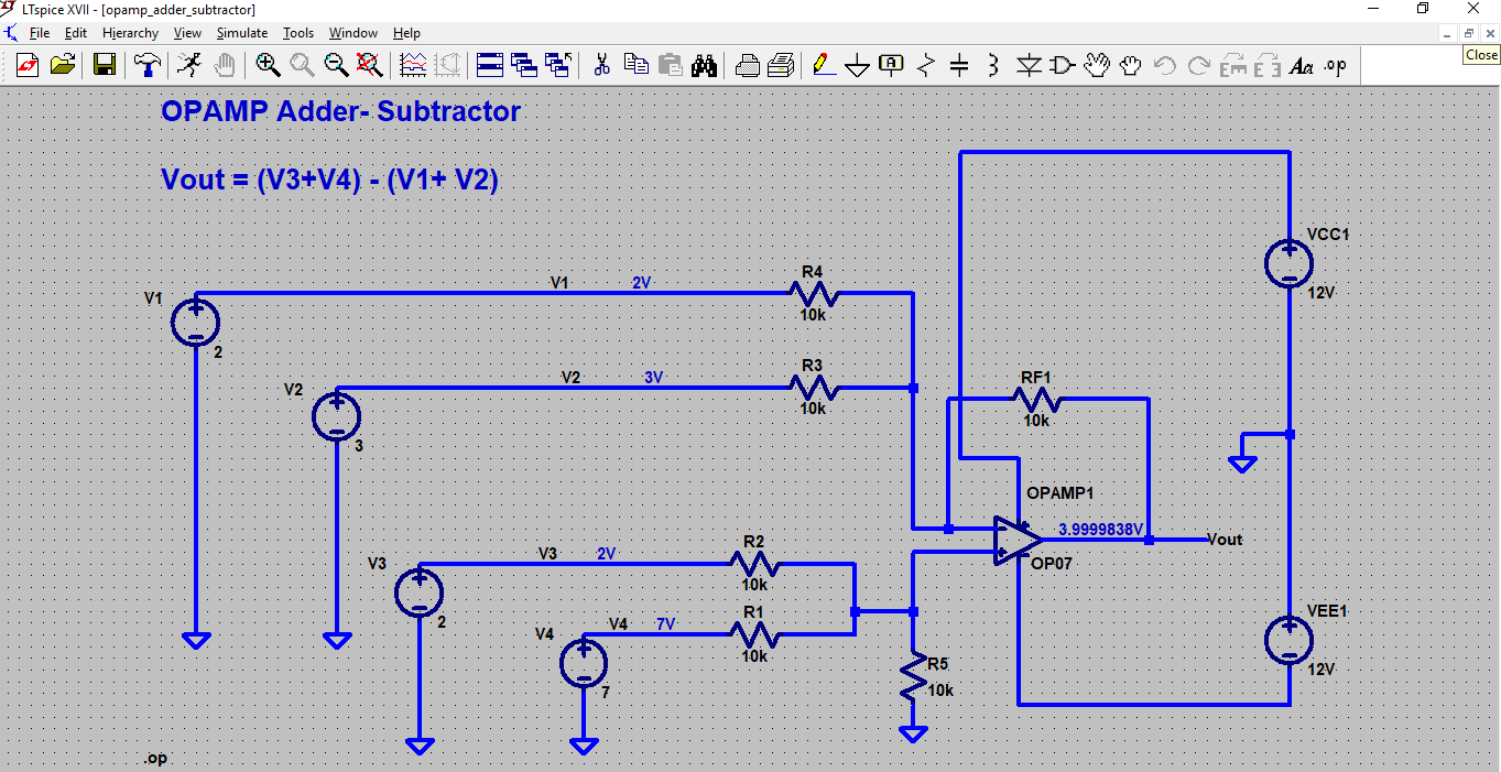
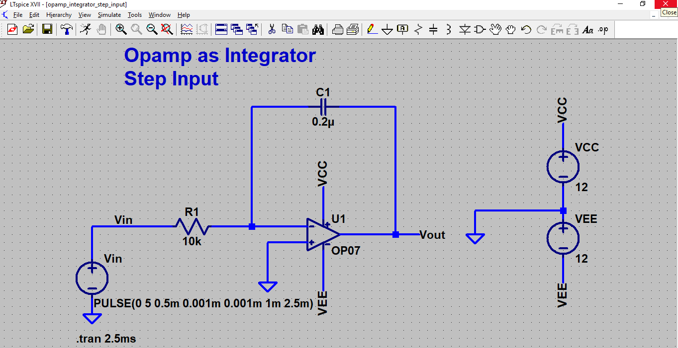
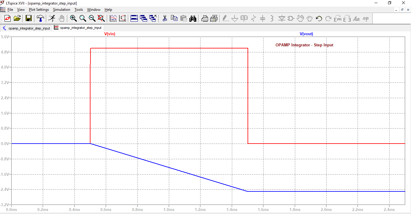
Topics Covered : Op-amp Integrator (revision), Step input applied to Integrator example, Op-amp Differentiator + small numerical, Op-amp as Adder- Subtractor, Simulation Schematics + Simulation shown in class for (Opamp Subtractor, Opamp Adder-Subtractor, Opamp Integrator, Opamp differentiator)
Topics Covered : Op-amp Integrator (revision), Step input applied to Integrator example, Op-amp Differentiator + small numerical, Op-amp as Adder- Subtractor, Simulation Schematics + Simulation shown in class for (Opamp Subtractor, Opamp Adder-Subtractor, Opamp Integrator, Opamp differentiator)
| licd_06.pdf |
Videos related to lecture 06 are below : 06.01 to 06.02 ( Total 2 )
Video 06.01 : Op-amp Differentiator
Video 06.02 : Demo of Op-amp Integrator and Differentiator with input as square wave
Observe the outputs for the same type of inputs for both.
Isn't it Interesting ?
Observe the outputs for the same type of inputs for both.
Isn't it Interesting ?
As promised whatever SIMULATIONS circuits we simulate in class live, will be shared from 26/7/2018 on-wards
Simulation of various circuits were carried out in LTSpice
Simulation of various circuits were carried out in LTSpice
SIMULATIONS related to lecture 06 are below : 06.01 to 06.06 ( Total 6 images)
SIMULATION 06.01: Op-amp Subtractor Schematic and output
SIMULATION 06.02: Op-amp Adder-Subtractor Schematic and output
SIMULATION 06.03: Op-amp Integrator(Ideal) Schematic with Step input
SIMULATION 06.04: Op-amp Integrator(Ideal) Output waveform with Step input
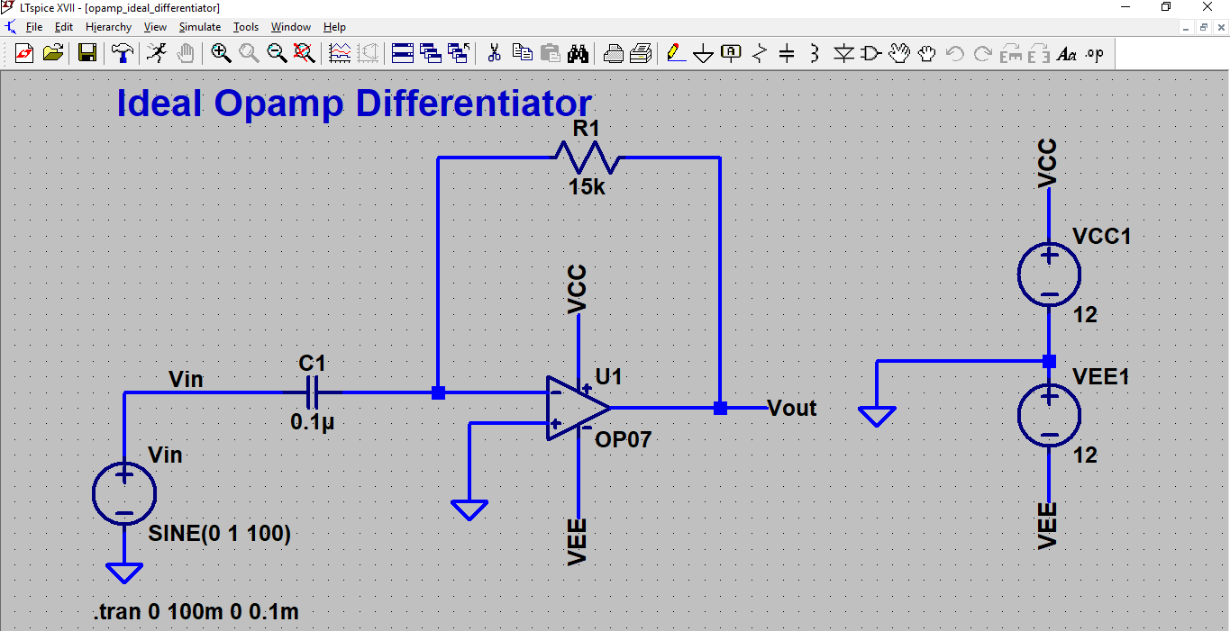
SIMULATION 06.05: Op-amp Differentiator(Ideal) Schematic with sine input
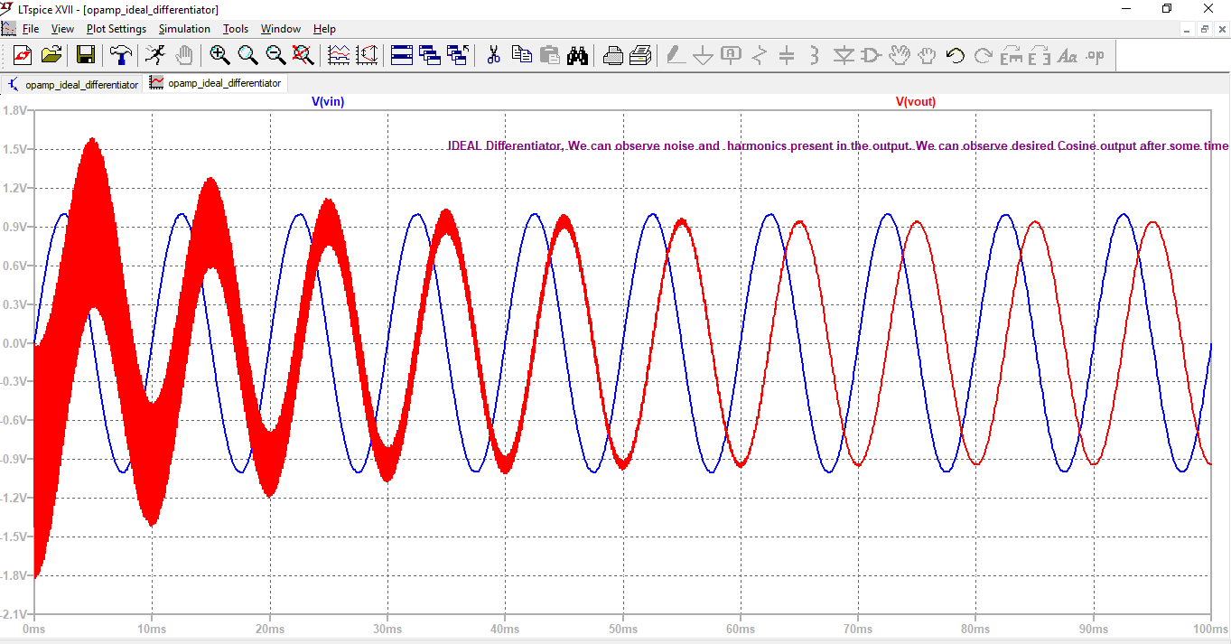
SIMULATION 06.06: Op-amp Differentiator(Ideal) Output waveform with sine input
Lecture 07 handout dated 26-07-2018
Topics Covered : Ideal Opamp Circuit analysis numericals (Two solved in class + 1 self study + Simulation of two solved numerical's), Idea to solve complex circuit around op-amp (One example circuit with Vo/V1 expression) ,
Topics Covered : Ideal Opamp Circuit analysis numericals (Two solved in class + 1 self study + Simulation of two solved numerical's), Idea to solve complex circuit around op-amp (One example circuit with Vo/V1 expression) ,
| licd_07.pdf |
SIMULATIONS related to lecture 07 are below : 07.01 to 07.05 ( Total 5 images)
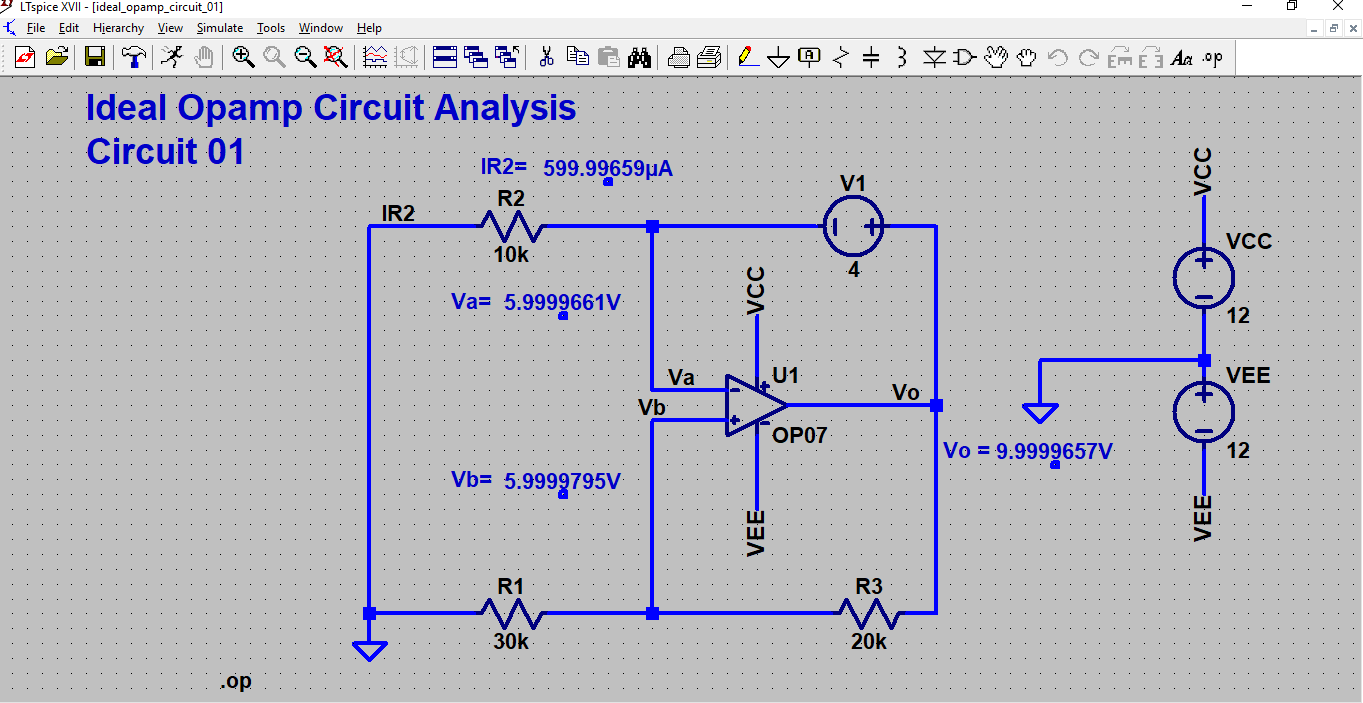
SIMULATION 07.01: Ideal Opamp circuit analysis (CIRCUIT 01)
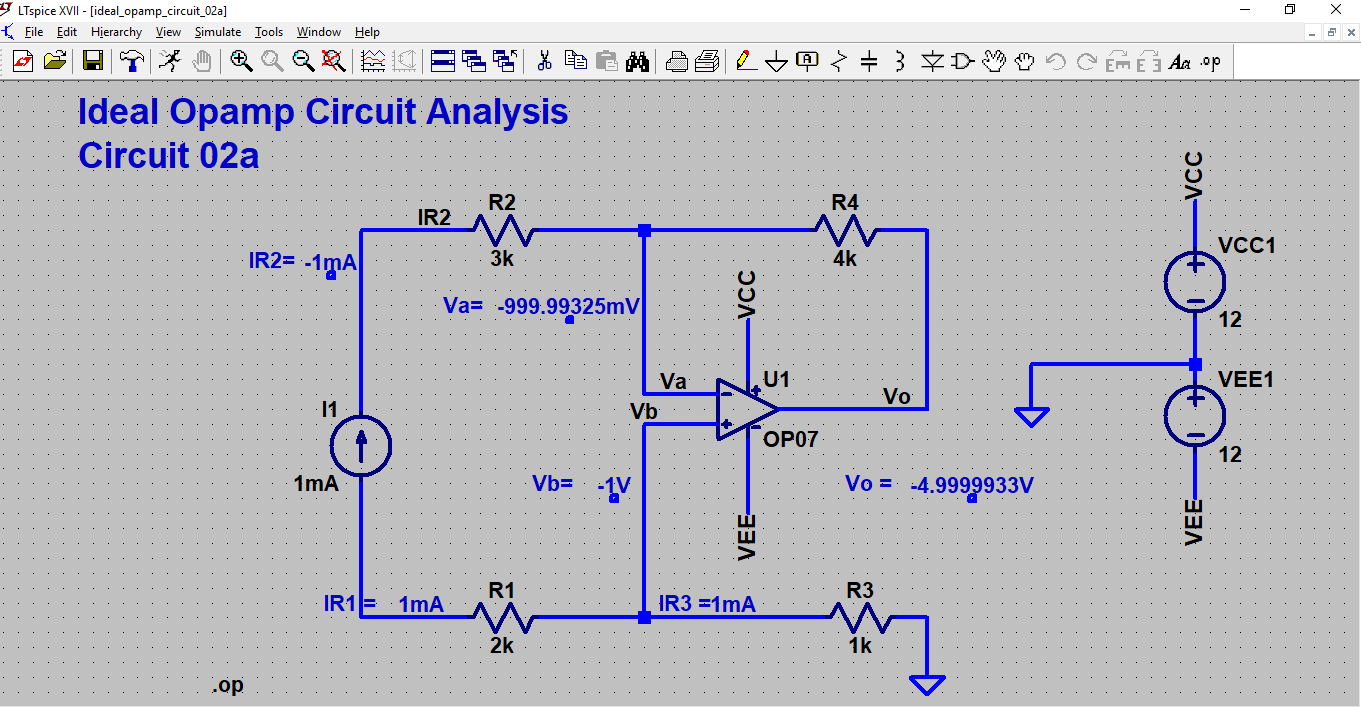
SIMULATION 07.02: Ideal Opamp circuit analysis (CIRCUIT 02a)
SIMULATION 07.03: Ideal Opamp circuit analysis (CIRCUIT 02b)
SIMULATION 07.04: Ideal Opamp circuit analysis (CIRCUIT 04a)
SIMULATION 07.05: Ideal Opamp circuit analysis (CIRCUIT 04b)
Lecture 08 handout dated 27-07-2018
Topics Covered : 3 opamp Instrumentation Amplifier gain derivation, Design of 3 opamp IA and its conceptual discussion of application (Temperature sensing and display)
Topics Covered : 3 opamp Instrumentation Amplifier gain derivation, Design of 3 opamp IA and its conceptual discussion of application (Temperature sensing and display)
| licd_08.pdf |
Announcement:
LICD Weekly Test 02 is active now
Test will remain active till 23:59 Hrs 29/7/2018
One can access the test via the link given below:
https://goo.gl/forms/KnwRvobn6t1EH0WB2
End of Week 02: 24-07-2018 to 27-07-2018
Total no. of Lectures conducted: 04
Total Hours: 04
Activities during week 02:
1) Numerical examples in LT Spice schematic and simulation tool
2) Use of LIVE Quiz in class
3) Weekly Test 02 conducted via Google assessment
4) Use of Curious Topic in Live class ( Exploring through the topic and then elaborating its existances and name)
Highlights: LICD Weekly Test 02
Total students: 07
LICD Weekly Test 02 is extended till 1st August
Test will remain active till 23:59 Hrs 1/8/2018
One can access the test via the link given below:
https://goo.gl/forms/KnwRvobn6t1EH0WB2
Since there is no official marks associated with this test, one can give this test to practice and apply concept learned in class
Test will remain active till 23:59 Hrs 1/8/2018
One can access the test via the link given below:
https://goo.gl/forms/KnwRvobn6t1EH0WB2
Since there is no official marks associated with this test, one can give this test to practice and apply concept learned in class
LICD Weekly Test 02 Solution will be uploaded by 2nd August 2018
| licd_weekly_test_2_solution.pdf |
Lecture 09 handout dated 31-07-2018
Topics Covered : Why Instrumentation Amplifier(I.A) , simple bridge circuit, definition of common-mode signal and CMRR, interfacing of bridge circuit with difference amplifier and observing the loading of bridge circuit, interfacing of Instrumentation amplifier with bridge circuit which overcomes the loading, Limitations of difference amplifier, Features like High input impedance and large variable gain of I.A
Piece of advice: Use this handout of licd_09.pdf along with Video 09.01, 09.02 and 09.03
| licd_09.pdf |
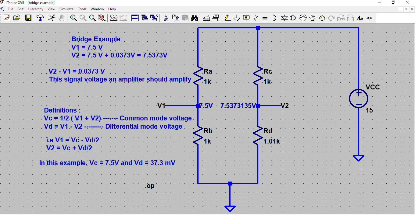
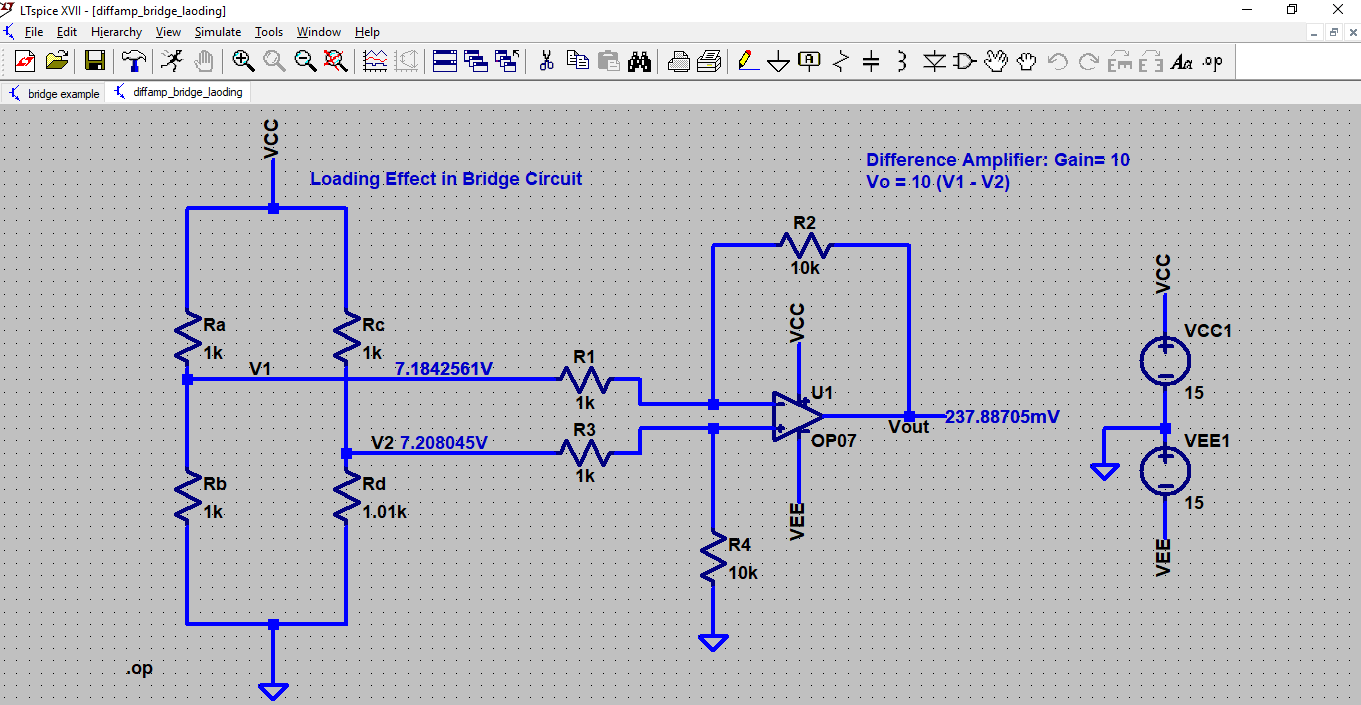
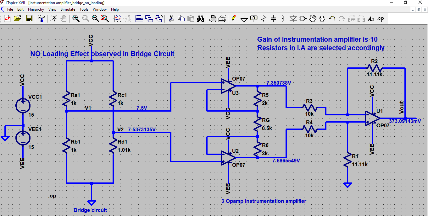
SIMULATIONS related to lecture 09 are below : 09.01 to 09.03 ( Total 3 images)
SIMULATION 09.01: Bridge Circuit and definitions of Common-mode voltage and differential mode-voltage
SIMULATION 09.02: Interfacing of Bridge Circuit and difference amplifier and observation of Loading effect
SIMULATION 09.03: Interfacing of Bridge Circuit with Instrumentation Amplifier
Videos related to lecture 09 are below : 09.01 to 09.03 ( Total 3 )
Video 09.01 : Op-amp Differential amplifier derivation, functionality and its limitations
Video 09.02 : Op-amp based Instrumentation amplifier ( Its need is well explained)
One can skip video from 10 minutes 30 seconds to 19 minutes 12 seconds.
One can skip video from 10 minutes 30 seconds to 19 minutes 12 seconds.
Video 09.03 : Op-amp based Instrumentation amplifier ( How CMRR is reduced in IA is explained)
One can watch the video to 10 minutes 40 seconds for Instrumentation topic only
One can watch the video to 10 minutes 40 seconds for Instrumentation topic only
Lecture 10 handout dated 01-08-2018
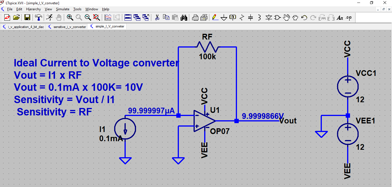
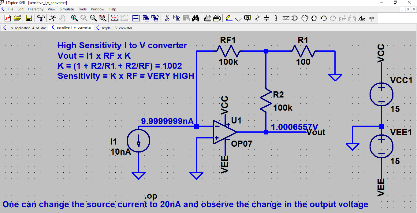
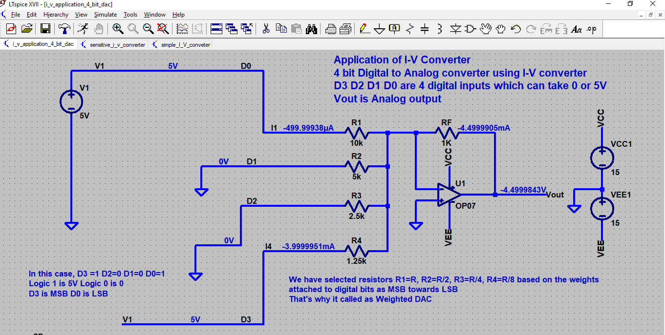
Topics Covered: Effect of Common-mode signal on differential amplifier and instrumentation amplifier, Simplified derivation of gain for 3 opamp Instrumentation Amplifier, concept of current to voltage conversion, I to V converter using OPAMP, Sensitivity definition for I to V converter, High Sensitivity Opamp based I-V converter ( only Concept + Simulation shown), 3 Application of I to V converter (in brief): 1) Using Photodiode 2) Using Photoconductive cell and 3) 4 bit Digital to Analog Converter (only simulation shown)
Topics Covered: Effect of Common-mode signal on differential amplifier and instrumentation amplifier, Simplified derivation of gain for 3 opamp Instrumentation Amplifier, concept of current to voltage conversion, I to V converter using OPAMP, Sensitivity definition for I to V converter, High Sensitivity Opamp based I-V converter ( only Concept + Simulation shown), 3 Application of I to V converter (in brief): 1) Using Photodiode 2) Using Photoconductive cell and 3) 4 bit Digital to Analog Converter (only simulation shown)
| licd_10.pdf |
SIMULATIONS related to lecture 10 are below : 10.01 to 10.03 ( Total 3 images)
SIMULATION 10.01: Ideal Current to Voltage Converter
SIMULATION 10.02: High Sensitivity Current to Voltage Converter
SIMULATION 10.02: 4 bit Digital to Analog converter
Videos related to lecture 10 are below : 10.01 ( Total 1 )
Video 10.01 : Current to Voltage converter and its applications
Lecture 11 handout dated 02-08-2018
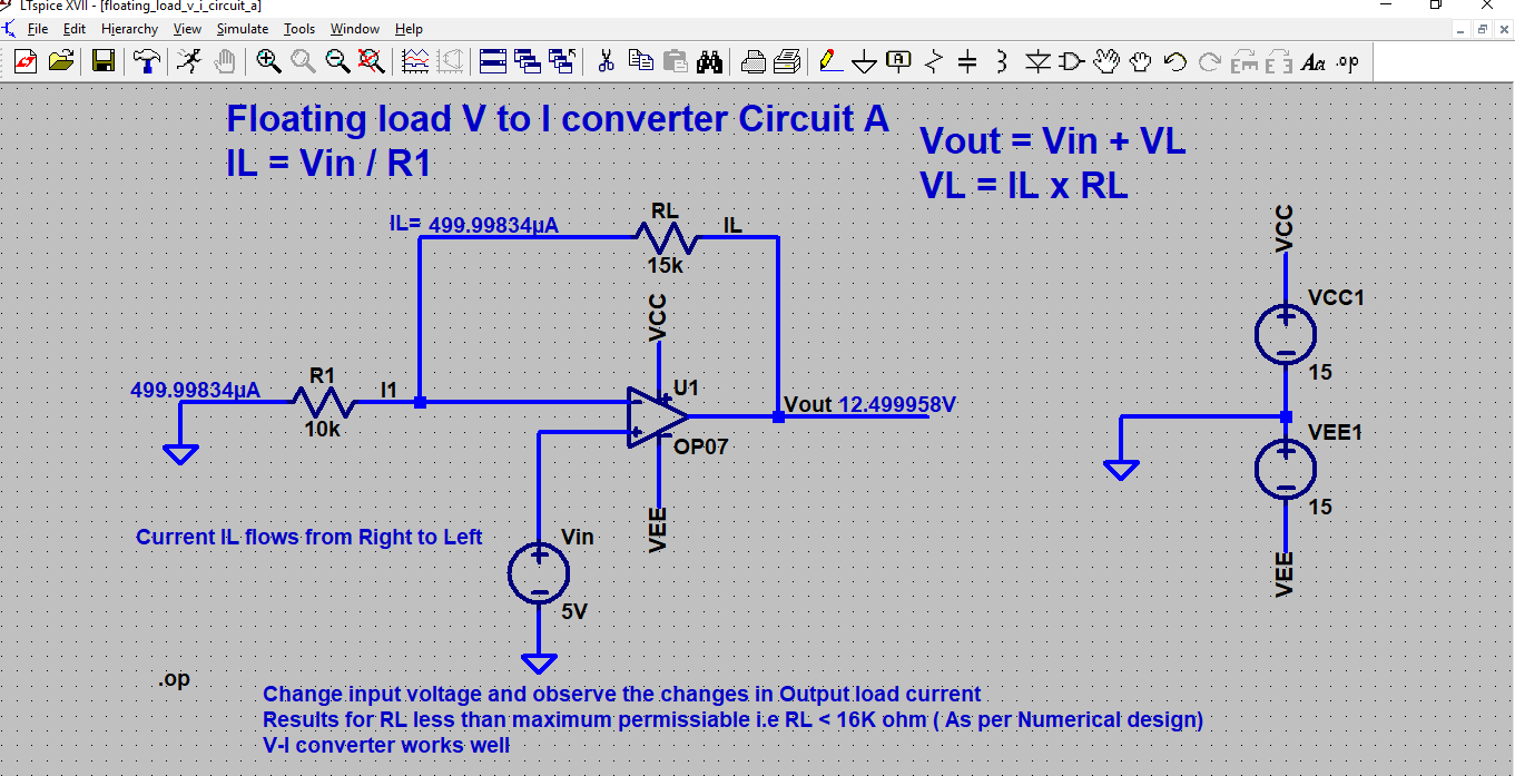
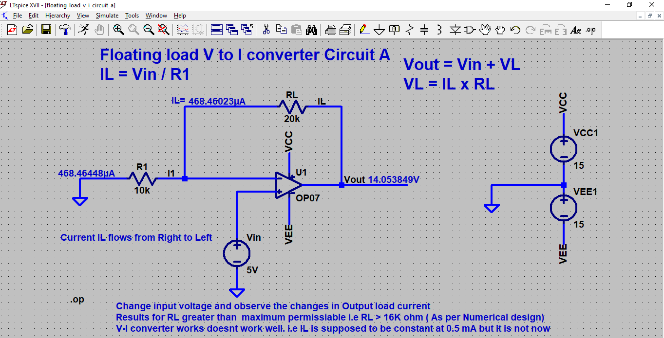
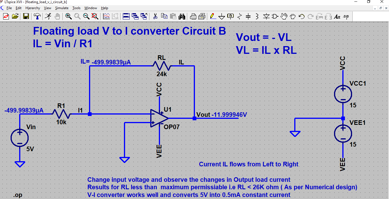
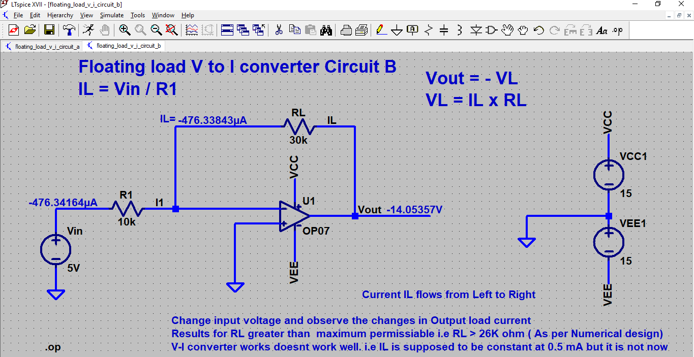
Topics Covered: Concept of current to voltage conversion, Floating load V to I converter using OPAMP, Application of V to I converter (in brief): 1) Driving an LED i.e test brightness of different LED's for constant current 2) To find the matched pairs of diodes or matched pair of Zener diodes, Voltage compliance concept, Quiz of 90 second i.e to find Io and Vout for given circuit, Numerical on floating load V-I converter and verification with simulation
Topics Covered: Concept of current to voltage conversion, Floating load V to I converter using OPAMP, Application of V to I converter (in brief): 1) Driving an LED i.e test brightness of different LED's for constant current 2) To find the matched pairs of diodes or matched pair of Zener diodes, Voltage compliance concept, Quiz of 90 second i.e to find Io and Vout for given circuit, Numerical on floating load V-I converter and verification with simulation
| licd_11.pdf |
SIMULATIONS related to lecture 11 are below : 11.01 to 11.04 ( Total 4 images)
SIMULATION 11.01: Floating load Voltage to current Converter w.r.t numerical in LICD 11 handout (Circuit A) ........ Here Circuit works well
SIMULATION 11.02: Floating load Voltage to current Converter w.r.t numerical in LICD 11 handout (Circuit A)..... Circuit doesn't work as max value of RL is exceeded
SIMULATION 11.03: Floating load Voltage to current Converter w.r.t numerical in LICD 11 handout (Circuit B)...... Here Circuit works well
SIMULATION 11.04: Floating load Voltage to current Converter w.r.t numerical in LICD 11 handout (Circuit B)..... Circuit doesn't work as max value of RL is exceeded
Videos related to lecture 11 are below : 11.01 ( Total 1 )
Video 11.01 : Voltage to current converter
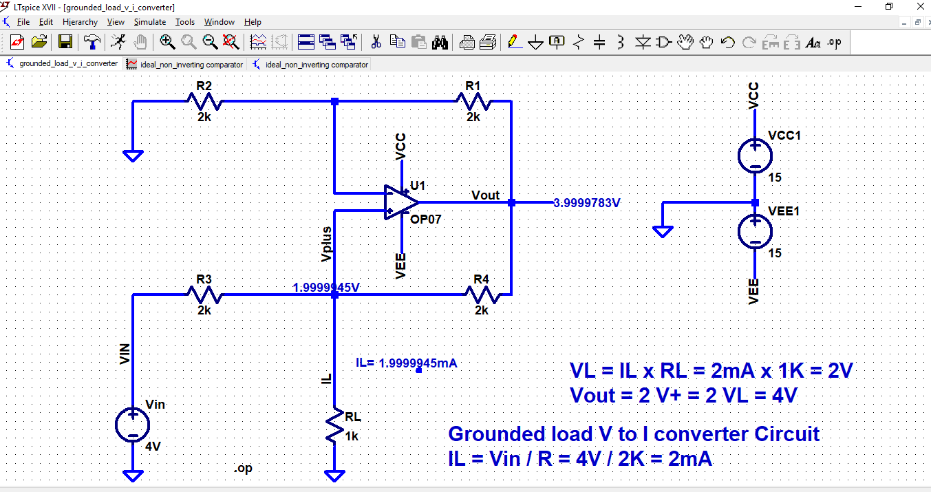
Lecture 12 handout dated 03-08-2018
Topics Covered: Grounded load V to I converter using OPAMP and verification of concept using simulation, Non-inverting comparator concept explained by simulating the circuit first, observing results in simulation real time, and interpretating them on green board, explaining the transfer characteristics of non-inverting comparator.
Assignment given to students : Draw input-output and transfer characteristics of inverting comparator with positive and negative reference voltage and of the non-inverting comparator with negative reference voltage.
| licd_12.pdf |
SIMULATIONS related to lecture 12 are below : 12.01 to 12.03 ( Total 3 images)
SIMULATION 12.01: Grounded load Voltage to current Converter with R=2k and RL=1k designed to convert 4 V to 2 mA
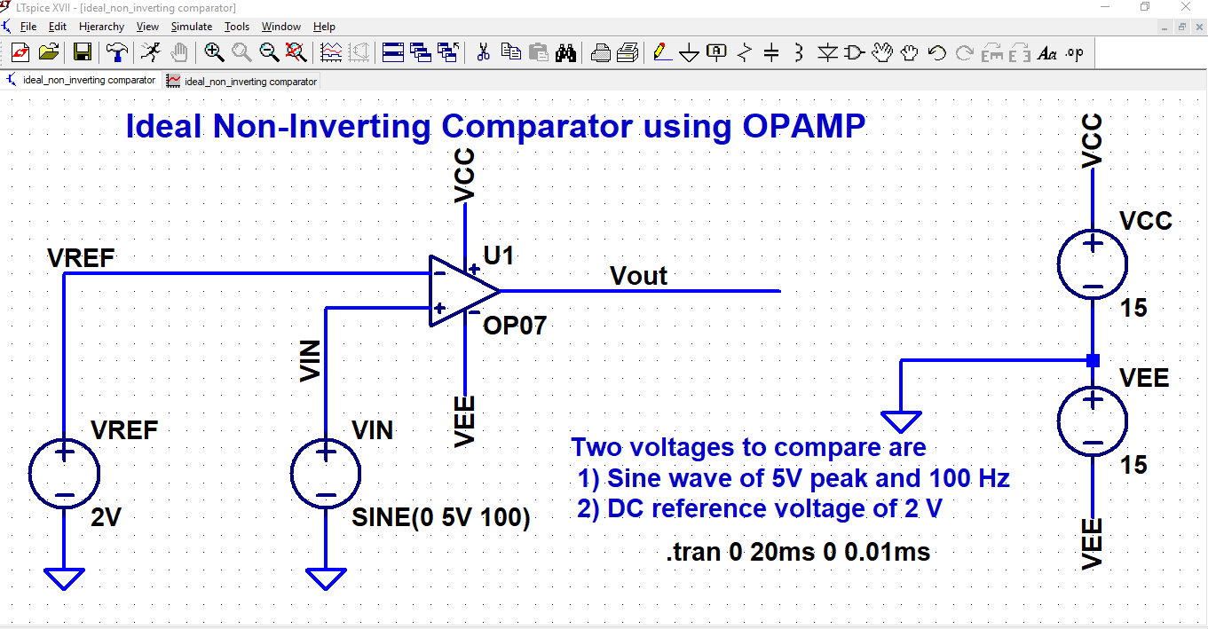
SIMULATION 12.02: Ideal Non-inverting Comparator using Op-amp with Vref=2V and Vin as a sine wave of 5V peak and 100Hz frequency
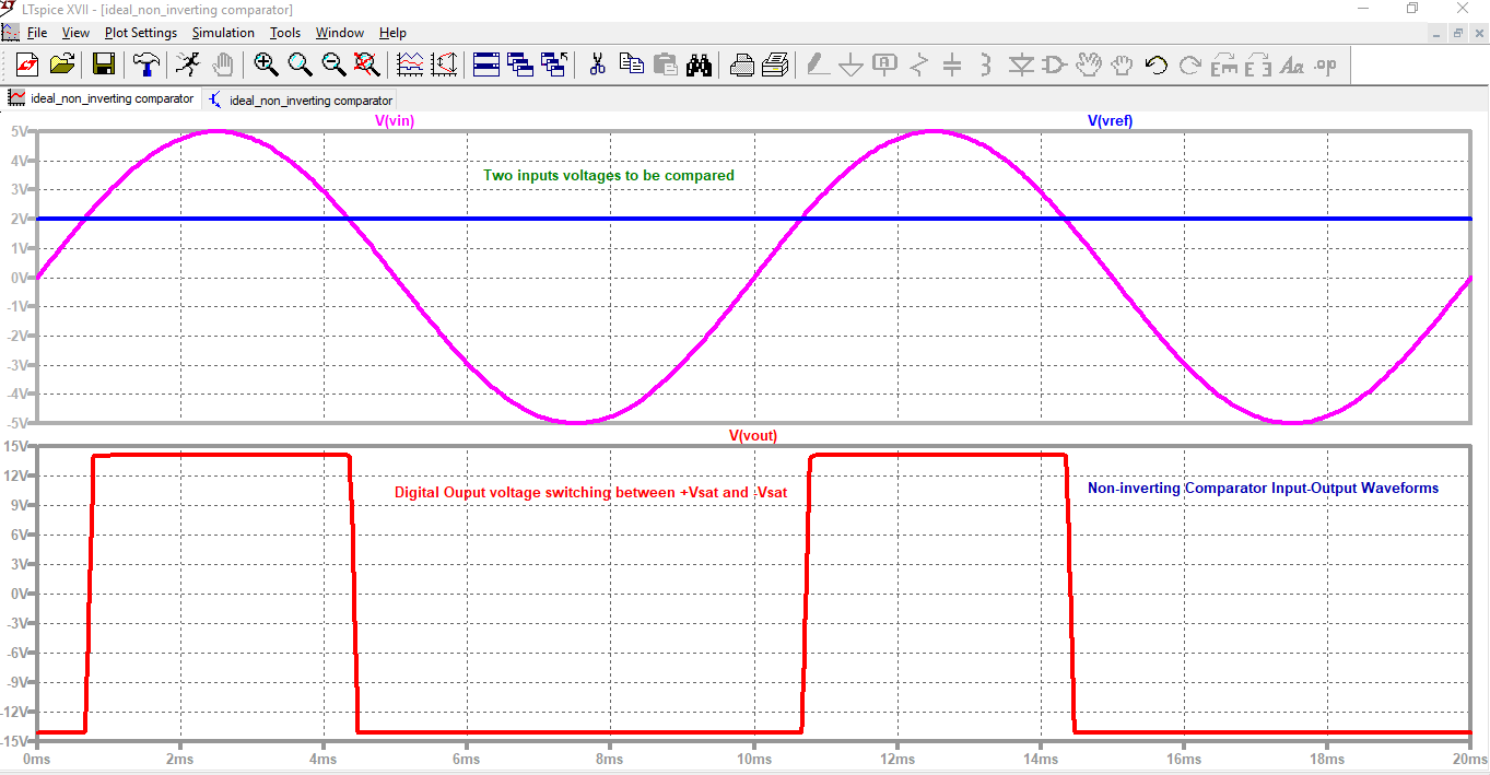
SIMULATION 12.03: Input-Output waveforms for Ideal Non-inverting Comparator
Announcement:
LICD Weekly Test 03 is active now
Test will remain active till 23:59 Hrs 06/08/2018
One can access the test via the link given below:
https://goo.gl/forms/ELOpImsbkd5PAYSn2
LICD Weekly Test 03 is active now
Test will remain active till 23:59 Hrs 06/08/2018
One can access the test via the link given below:
https://goo.gl/forms/ELOpImsbkd5PAYSn2
End of Week 03: 31-07-2018 to 03-08-2018
Total no. of Lectures conducted: 04
Total Hours: 04
Activities during week 03:
1) Concepts: Demonstrated in LT Spice schematic and simulation tool
2) Numerical examples: Demonstrated in LT Spice schematic and simulation tool
3) Use of LIVE Quiz in class
4) Weekly Test 03 conducted via Google assessment
4) WHY, HOW and WHERE approach (for circuits) was adopted in Live class
Highlights: LICD Weekly Test 03
Total students: 07
Lecture 13 handout dated 07-08-2018
Topics Covered: Inverting comparator: working + input-output waveforms + transfer characteristics, a look at practical comparator circuit, comparator bounded output using zener, Negative Vs Positive feedback, Analogy of a bowl and a marble, Application of a Comparator: Zero crossing Detector (ZCD), Limitation of ZCD
Mistake committed during lecture: Drawn transfer characteristics of ZCD incorrectly
NOTE: As promised in class, the derivation for Positive feedback circuit is uploaded in the form of videos 13.02 and 13.03 ( SHARED JUST FOR REFERENCE)
| licd_13.pdf |
Videos related to lecture 13 are below : 13.01 to 13.04 ( Total 4 )
Video 13.01 : Negative Vs Positive feedback
Video 13.02 : Positive feedback circuit using opamp
Video 13.03 : Derivation of Output voltage for Positive feedback circuit using opamp
Video 13.04 : OPAMP as comparator: ZERO Crossing Detector, it's usefulness and it's limitations
Lecture 14 handout dated 08-08-2018
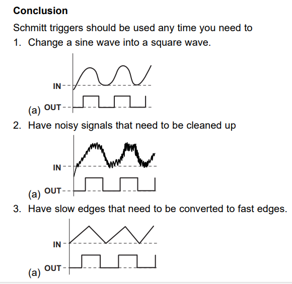
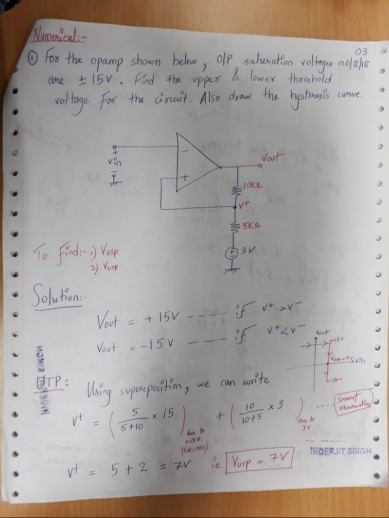
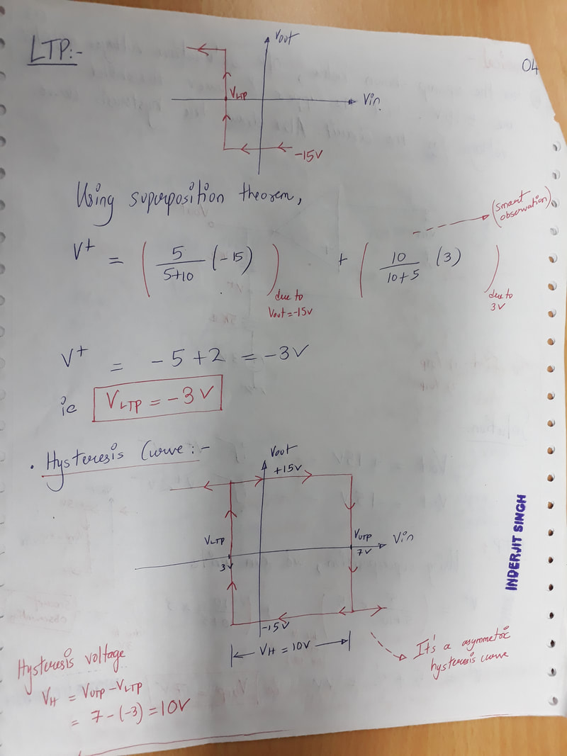
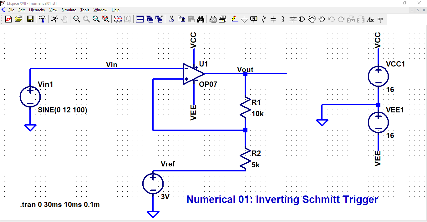
Topics Covered: Inverting Schmitt Trigger detailed analysis and working with numbers, Hysteresis curve, State diagram and input-output waveforms, Design of symmetric Schmitt Trigger with Vutp=5V and Vltp=-5V , Implementation of inverting schmitt trigger circuit and simulation results were demonstrated and discussed live in class.
NOTE: 1) Videos 14.01 to 14.03 are of inverting schmitt trigger explained w.r.t assumed values of R1, R2, supply voltage and saturation voltages
2) Material related to above videos 14.01 to 14.03 in licd_14.pdf is from page no. 1 to 7
3) The material in 1) and 2) serve as a base to understand Schmitt Triggers in simplest of form
4) Relevant material related to Schmitt trigger can be found from page no. 8 onwards ( This is what is expected to be written)
| licd_14.pdf |
Videos related to lecture 14 are below : 14.01 to 14.03 ( Total 3 )
Video 14.01 : Inverting Schmitt Trigger working and Analysis part 1
Video 14.02 : Inverting Schmitt Trigger working and Analysis part 2
Video 14.03 : Inverting Schmitt Trigger Hysteresis Curve and State Diagram
SIMULATIONS related to lecture 14 are below : 14.01 to 14.05 ( Total 5 images)
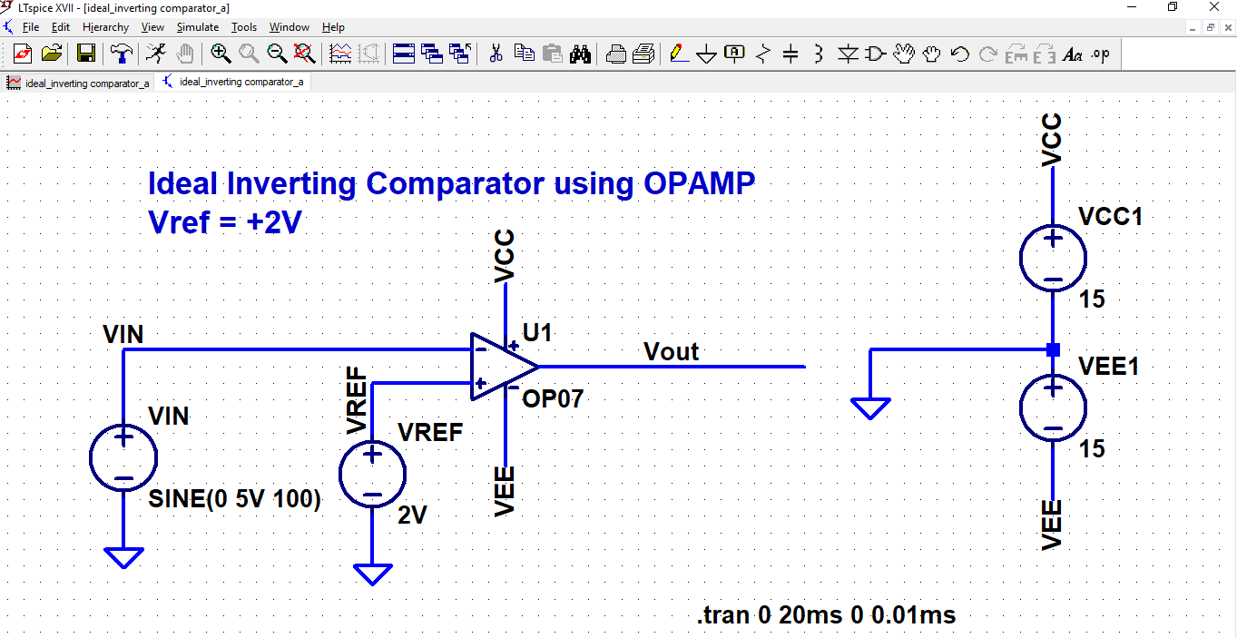
SIMULATION 14.01: Ideal Inverting Comparator using Op-amp with Vref=2V and Vin as a sine wave of 5V peak and 100Hz frequency
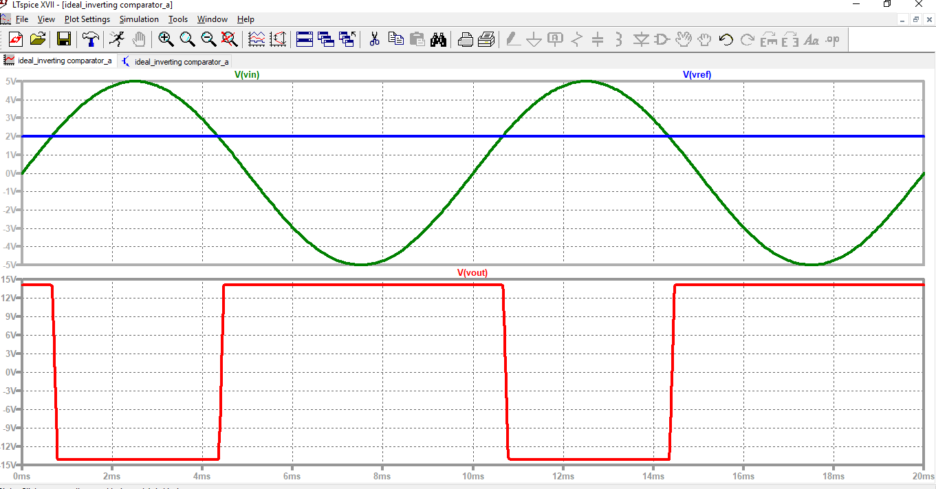
SIMULATION 14.02: Ideal Inverting Comparator Input-output Waveforms
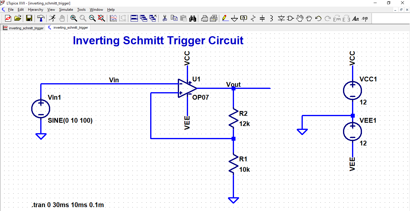
SIMULATION 14.03: Inverting Schmitt Trigger Circuit
Modifications: In class, while we simulated the circuit, we got the results which started with assumption that Vout is -Vsat, now since we assumed in class for inverting Schmitt trigger that lets assume output starts with +Vsat, that's the reason for modification
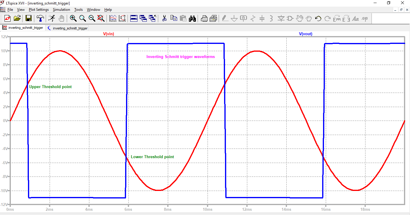
SIMULATION 14.04: Input- Output waveforms for Inverting Schmitt Trigger Circuit
Adjustment in simulation were done in order to be in consistent with waveforms discussed in class
SIMULATION 14.04: Input- Output waveforms for Inverting Schmitt Trigger Circuit
Adjustment in simulation were done in order to be in consistent with waveforms discussed in class
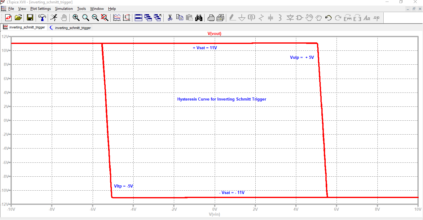
SIMULATION 14.05: Hysteresis Curve for Inverting Schmitt Trigger Circuit
Adjustment in simulation were done in order to be in consistent with waveforms discussed in class
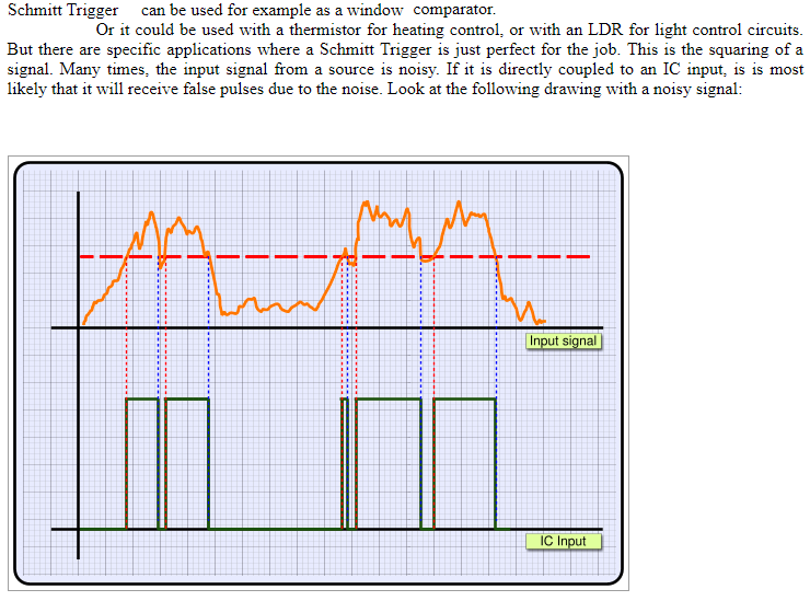
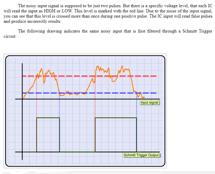
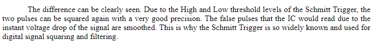
Limitation of Comparator and Usefulness of Schmitt Trigger (JUST for Info)
Lecture dated 09-08-2018: Not conducted
Make-up Lecture 01:
Since the lecture did'nt happen: Some contents are being shared, kindly note it in your books in order to compensate for the time lost.
Make-up Lecture 01:
Since the lecture did'nt happen: Some contents are being shared, kindly note it in your books in order to compensate for the time lost.
Numerical 01.01 :
Numerical 01.02 :
Simulation 01.01 :
Simulation 01.02 :
Lecture 15 handout dated 10-08-2018
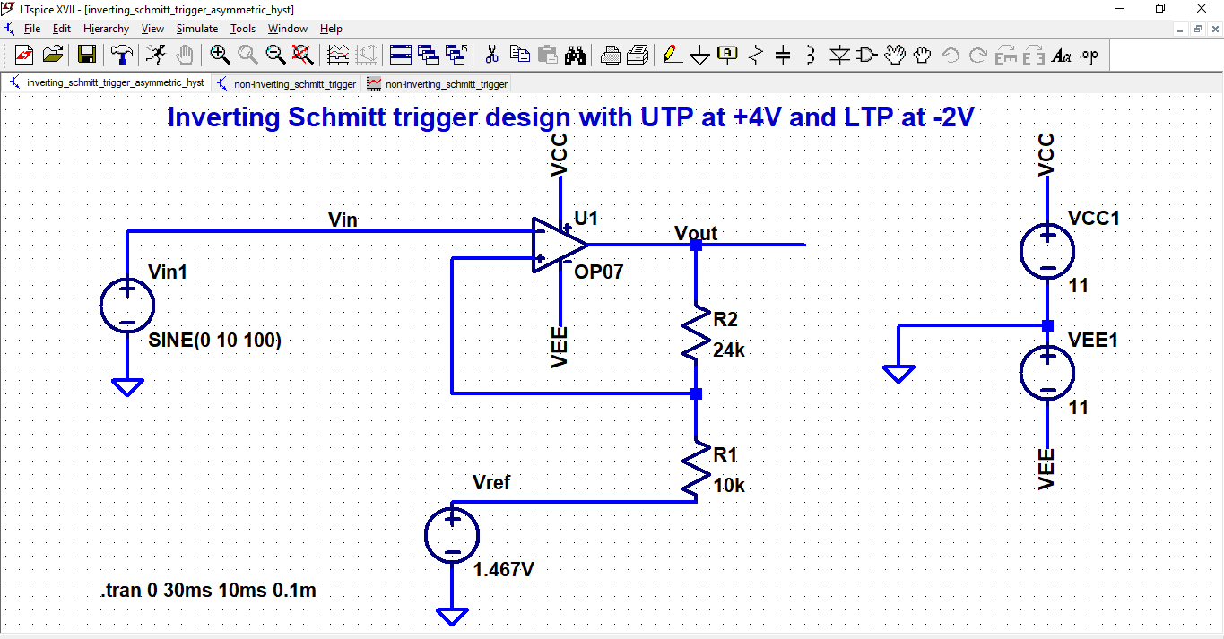
Topics Covered: Non-Inverting Schmitt Trigger (unsatisfied) analysis and working with boring equations, Hysteresis curve and input-output waveforms, Design of asymmetric inverting Schmitt Trigger with Vutp=+4V and Vltp=-2V , Implementation of non-inverting schmitt trigger circuit (made more sense), design of aysmmetric inverting Schmitt trigger with Reference voltage and with diode in LT Spice. Simulation results were demonstrated of all three circuits and discussed live in class.
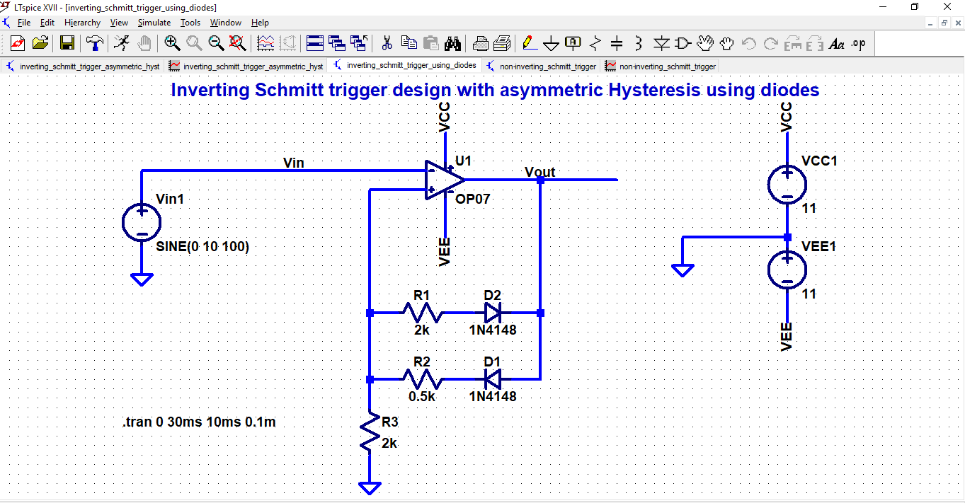
Topics not covered: Design of Asymmetric inverting schmitt trigger with diodes was NOT covered in class, but circuit was simulated and its results were observed in LT Spice simulation tool. Students are encouraged to ask doubts related to uncovered topic.
Topics Covered: Non-Inverting Schmitt Trigger (unsatisfied) analysis and working with boring equations, Hysteresis curve and input-output waveforms, Design of asymmetric inverting Schmitt Trigger with Vutp=+4V and Vltp=-2V , Implementation of non-inverting schmitt trigger circuit (made more sense), design of aysmmetric inverting Schmitt trigger with Reference voltage and with diode in LT Spice. Simulation results were demonstrated of all three circuits and discussed live in class.
Topics not covered: Design of Asymmetric inverting schmitt trigger with diodes was NOT covered in class, but circuit was simulated and its results were observed in LT Spice simulation tool. Students are encouraged to ask doubts related to uncovered topic.
| licd_15.pdf |
SIMULATIONS related to lecture 15 are below : 15.01 to 15.07 ( Total 7 images)
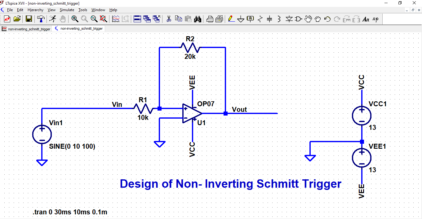
SIMULATION 15.01: Non-Inverting Schmitt Trigger Circuit
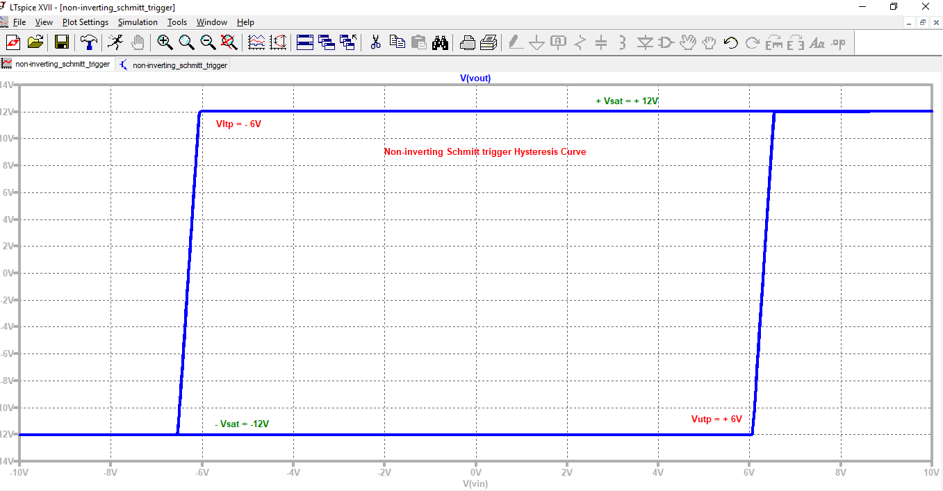
SIMULATION 15.02 : Hysteresis Curve for Non-Inverting Schmitt Trigger Circuit
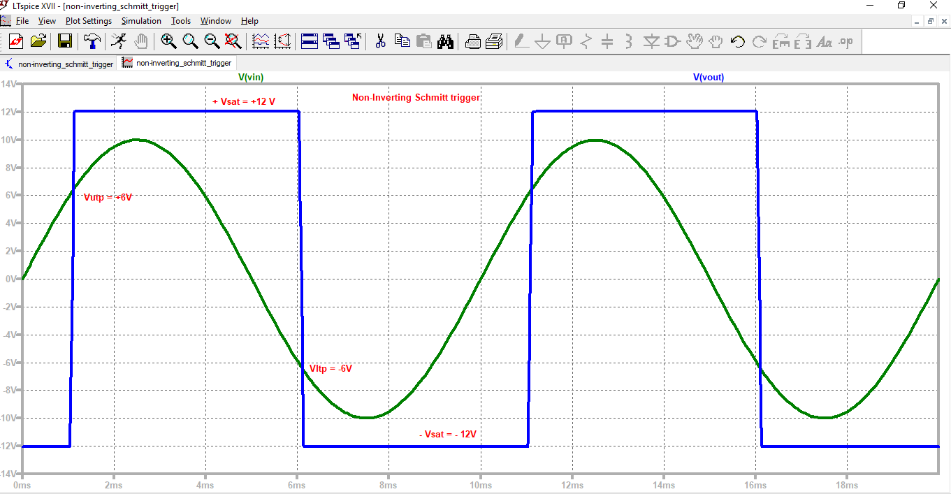
SIMULATION 15.03 : Input-Output Waveforms for Non-Inverting Schmitt Trigger Circuit
SIMULATION 15.03 : Input-Output Waveforms for Non-Inverting Schmitt Trigger Circuit
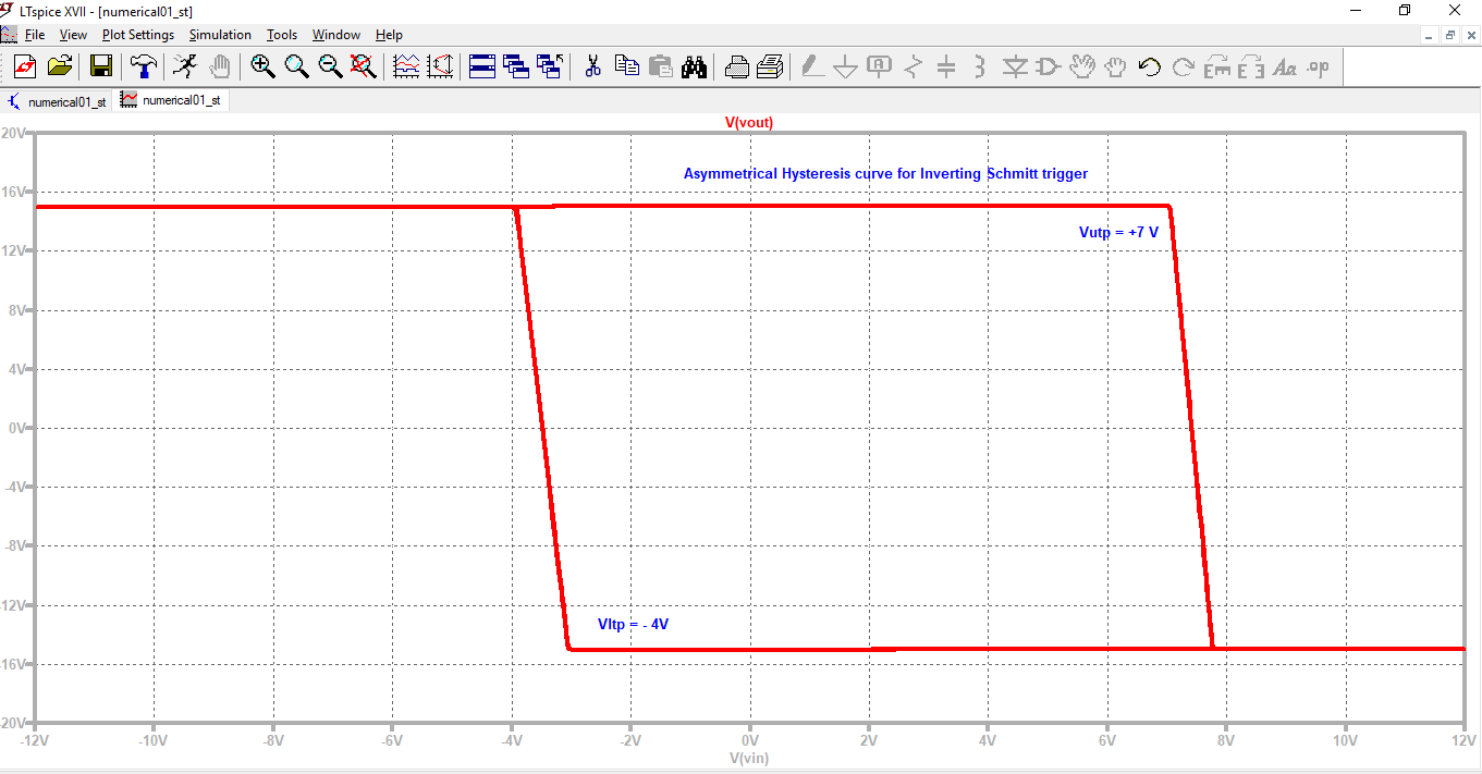
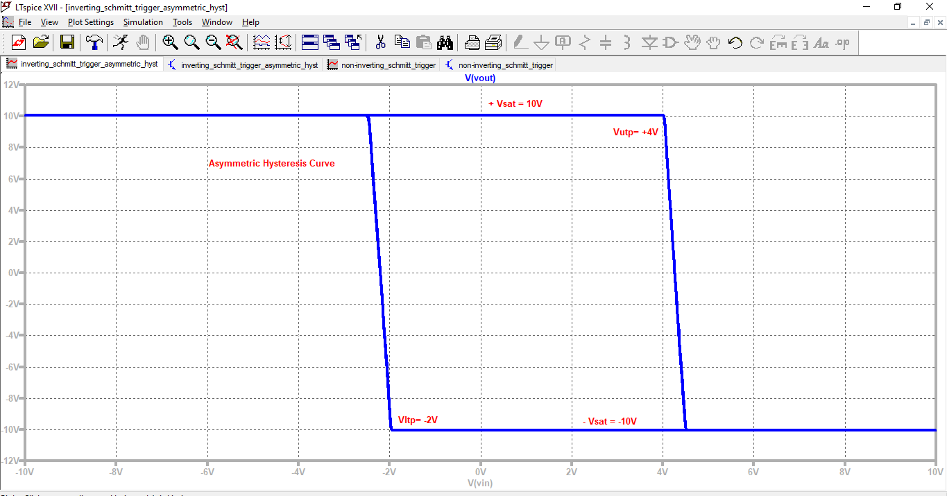
SIMULATION 15.04: Design of Asymmetric Inverting Schmitt Trigger Circuit with Vutp = 4V and Vltp = -2V
SIMULATION 15.05: Hysteresis for Inverting Schmitt Trigger Circuit with Vutp = 4V and Vltp = -2V
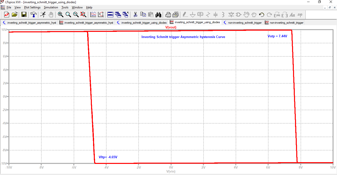
SIMULATION 15.06: Design of Asymmetric Inverting Schmitt Trigger Circuit using diodes
SIMULATION 15.07: Hysteresis for Asymmetric Inverting Schmitt Trigger Circuit using diodes
Announcement:
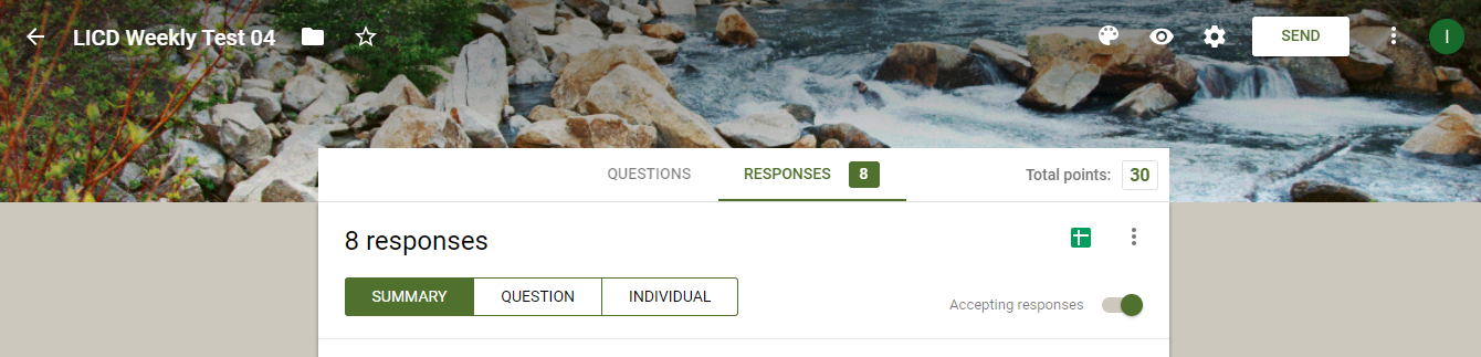
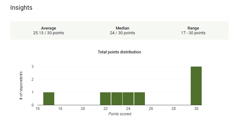
LICD Weekly Test 04 is active now
Test will remain active till 23:59 Hrs 12/08/2018
One can access the test via the link given below:
https://goo.gl/forms/VabmBrHAOUWL95w83
Highlights: LICD Weekly Test 04
Total students: 08
Total students: 08
End of Week 04: 07-08-2018 to 10-08-2018
Total no. of Lectures conducted: 03
Total Hours: 03
Activities during week 04:
1) Concepts: Demonstrated in LT Spice schematic and simulation tool
2) Numerical examples: Demonstrated in LT Spice schematic and simulation tool
3) Use of LIVE Quiz in class
4) Weekly Test 04 conducted via Google assessment
5) WHY, HOW and WHERE approach (for circuits) was adopted in Live class
6) Use of Analogy examples to explain difficult topics
Miscellaneous Video 01.01: Excellent working and analysis of Non-inverting Schmitt trigger and inverting Schmitt trigger
For Non-inverting schmitt trigger: Start video from 15 minutes and 22 seconds and watch it till the end.
For Non-inverting schmitt trigger: Start video from 15 minutes and 22 seconds and watch it till the end.
Lecture 16 handout dated 14-08-2018
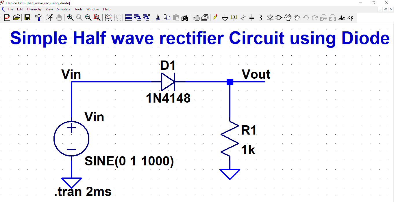
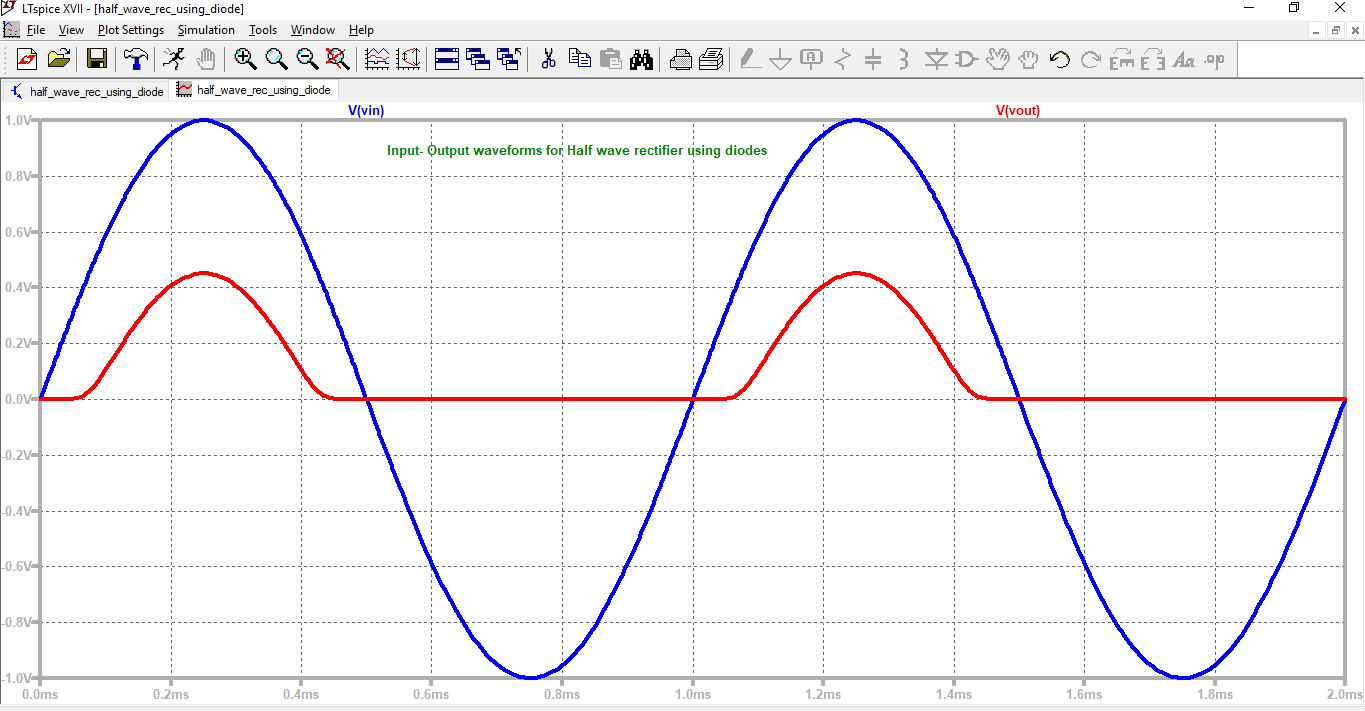
Topics Covered: Simple half wave rectifier incapability to rectify small signals explored with simulations, Precision half wave rectifier circuit analysis, transfer characteristics and input-output wave forms, Limitations associated with Precision half wave rectifier circuit were discussed. Simulation results were demonstrated and discussed live in class of the same.
Topics Covered: Simple half wave rectifier incapability to rectify small signals explored with simulations, Precision half wave rectifier circuit analysis, transfer characteristics and input-output wave forms, Limitations associated with Precision half wave rectifier circuit were discussed. Simulation results were demonstrated and discussed live in class of the same.
| licd_16.pdf |
Video related to lecture 16 is below : 16.01 ( Total 1 )
Video 16.01 : Application of Precision rectifier: AM demodulation
Start video from 9 minutes and 7 seconds and watch it till 16 minutes and 38 seconds
Start video from 9 minutes and 7 seconds and watch it till 16 minutes and 38 seconds
SIMULATIONS related to lecture 16 are below : 16.01 to 16.08 ( Total 8 images)
SIMULATION 16.01: Simple Half wave rectifier circuit using diodes
SIMULATION 16.02: Input- Output waveform's for Simple Half wave rectifier using diodes
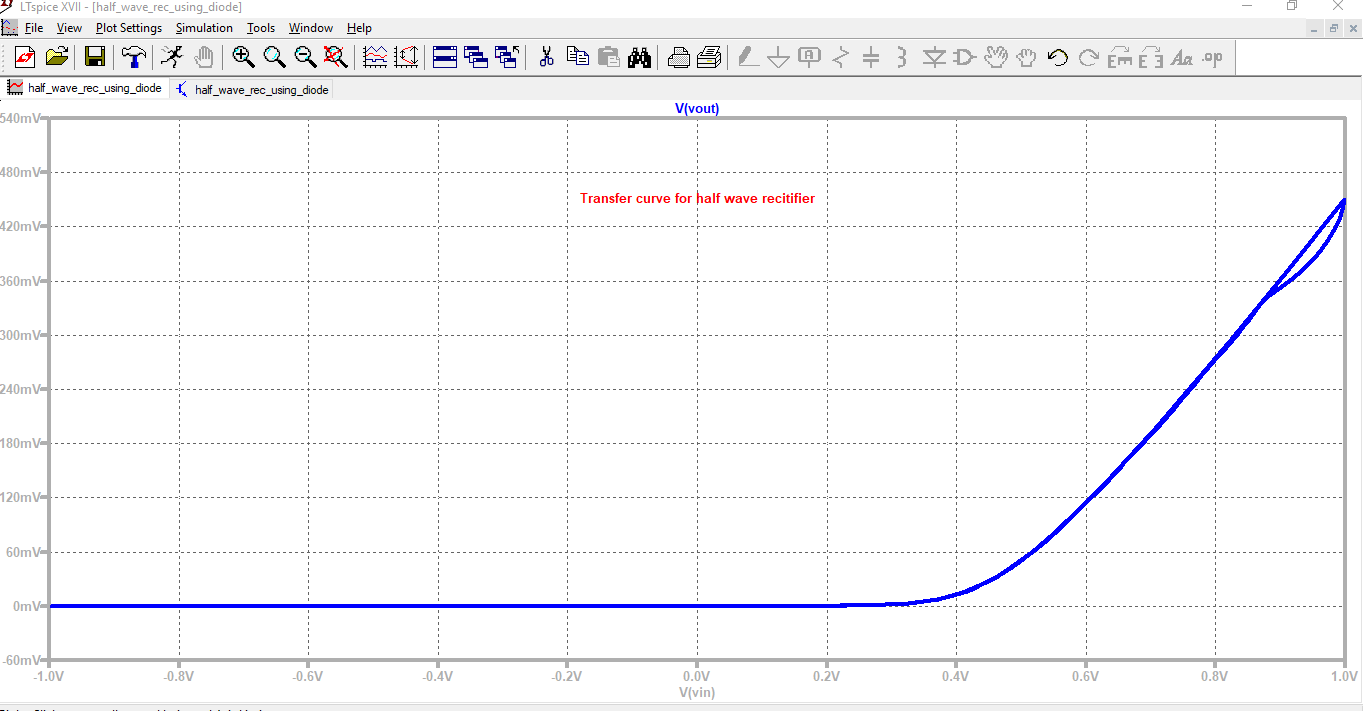
SIMULATION 16.03: Transfer curve for Simple Half wave rectifier using diodes
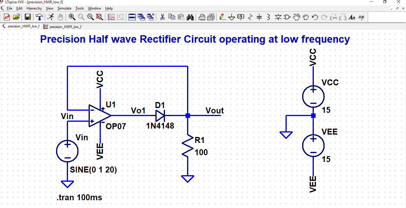
SIMULATION 16.04: Precision Half wave rectifier circuit
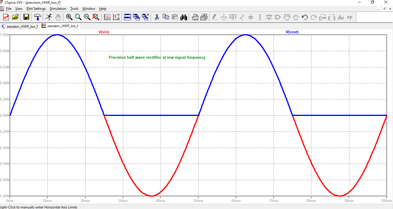
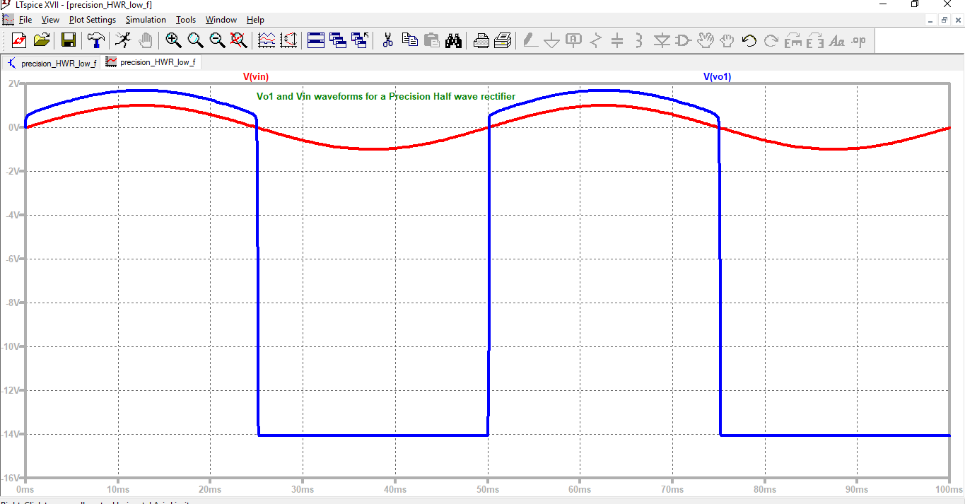
SIMULATION 16.05: Input- Output waveform's for Precision Half wave rectifier circuit
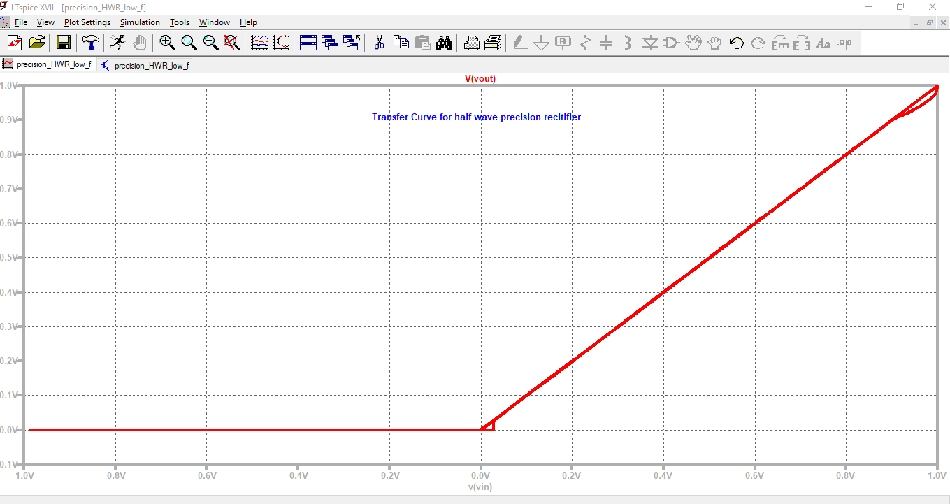
SIMULATION 16.06: Transfer curve for Precision Half wave rectifier circuit
SIMULATION 16.07: Opamp output Vo1 waveforms showing negative saturation for Precision Half wave rectifier circuit
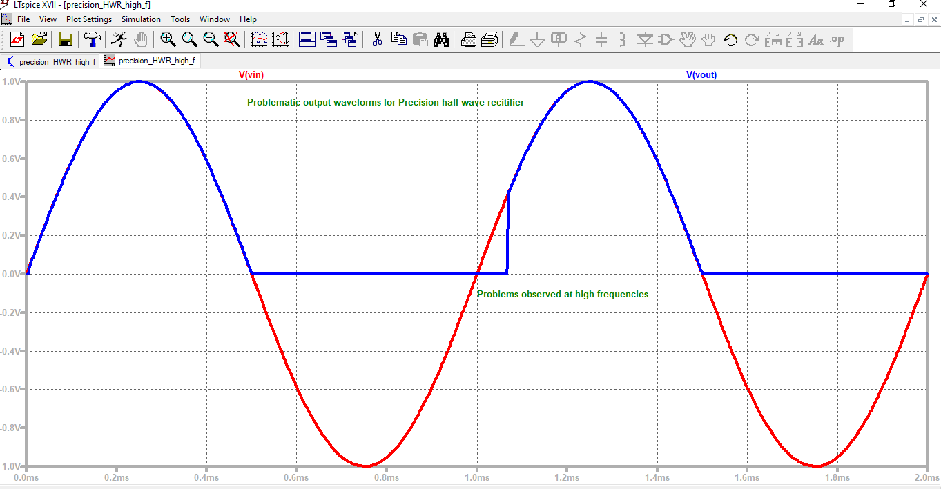
SIMULATION 16.08: Distortion in the output waveform's when Precision Half wave rectifier is operating at high frequency
Lecture 17 handout dated 16-08-2018
Topics Covered: Revision of precision half wave rectifier, Improved Precision half wave rectifier analysis, input-output characteristics, transfer curve. Simulation results for Improved half-wave precision rectifier were demonstrated and discussed live in class, 90 Second quiz was floated in class live, and its results were shown in LT Spice simulation tool, Concept building of Full- wave Precision rectifier using half wave precision rectifier and inverting summer and simulation results of the same were discussed live in class, A textbook based Precision Full-wave rectifier was discussed in class in a JET- like speed during dying moments of the lecture.
Topics Covered: Revision of precision half wave rectifier, Improved Precision half wave rectifier analysis, input-output characteristics, transfer curve. Simulation results for Improved half-wave precision rectifier were demonstrated and discussed live in class, 90 Second quiz was floated in class live, and its results were shown in LT Spice simulation tool, Concept building of Full- wave Precision rectifier using half wave precision rectifier and inverting summer and simulation results of the same were discussed live in class, A textbook based Precision Full-wave rectifier was discussed in class in a JET- like speed during dying moments of the lecture.
| licd_17.pdf |
SIMULATIONS related to lecture 17 are below : 17.01 to 17.10 ( Total 10 images)
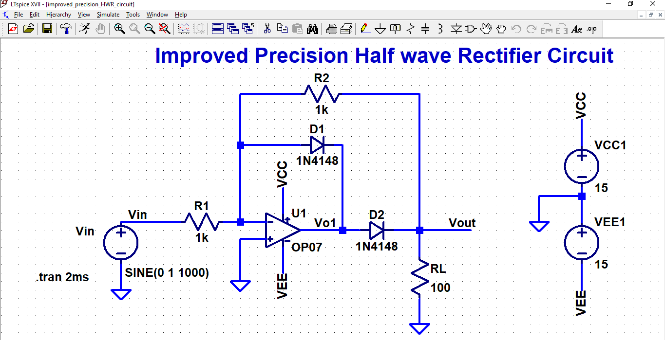
SIMULATION 17.01: Improved Precision Half wave rectifier circuit 1
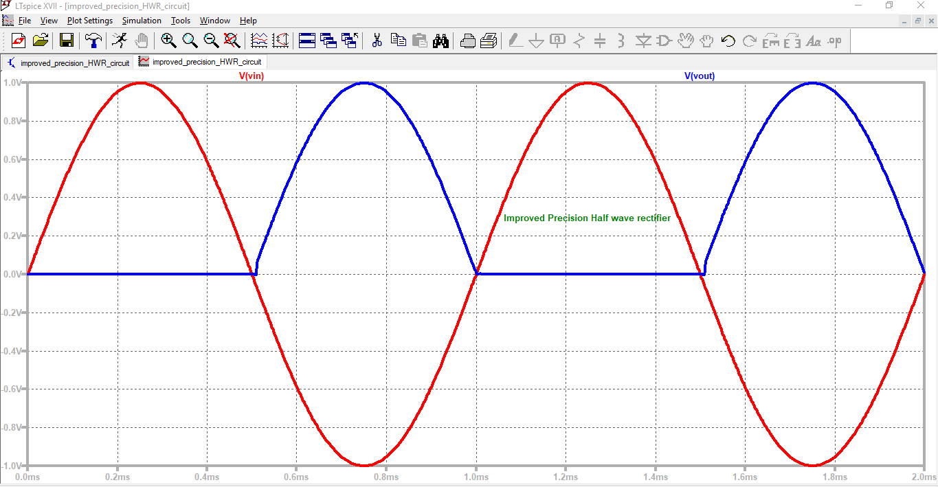
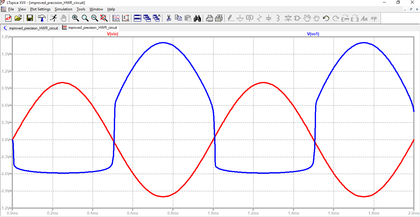
SIMULATION 17.02: Input-Output waveform's for Improved Precision Half wave rectifier circuit 1
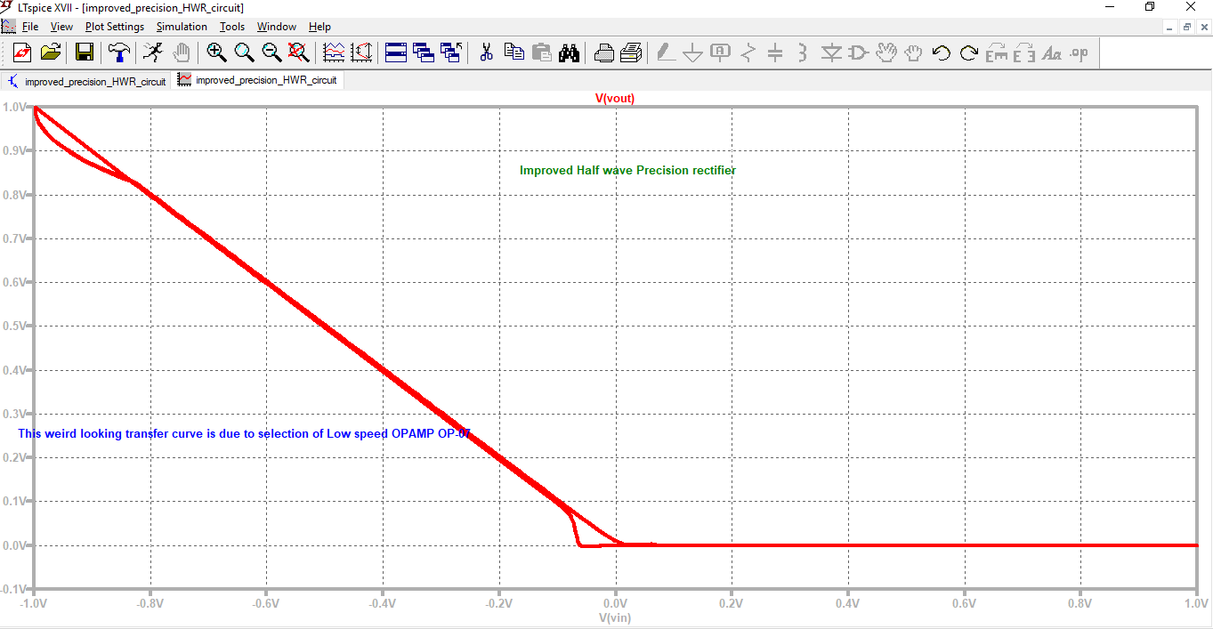
SIMULATION 17.03: Transfer curve for Improved Precision Half wave rectifier circuit 1
SIMULATION 17.04: Opamp output Vo1 waveforms showing that opamp never enter's saturation regime
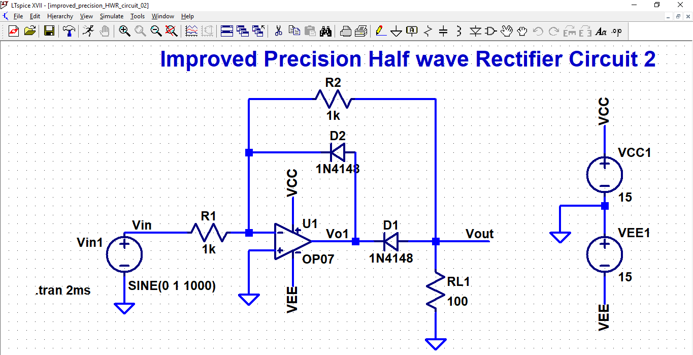
SIMULATION 17.05: Improved Precision Half wave rectifier circuit 2
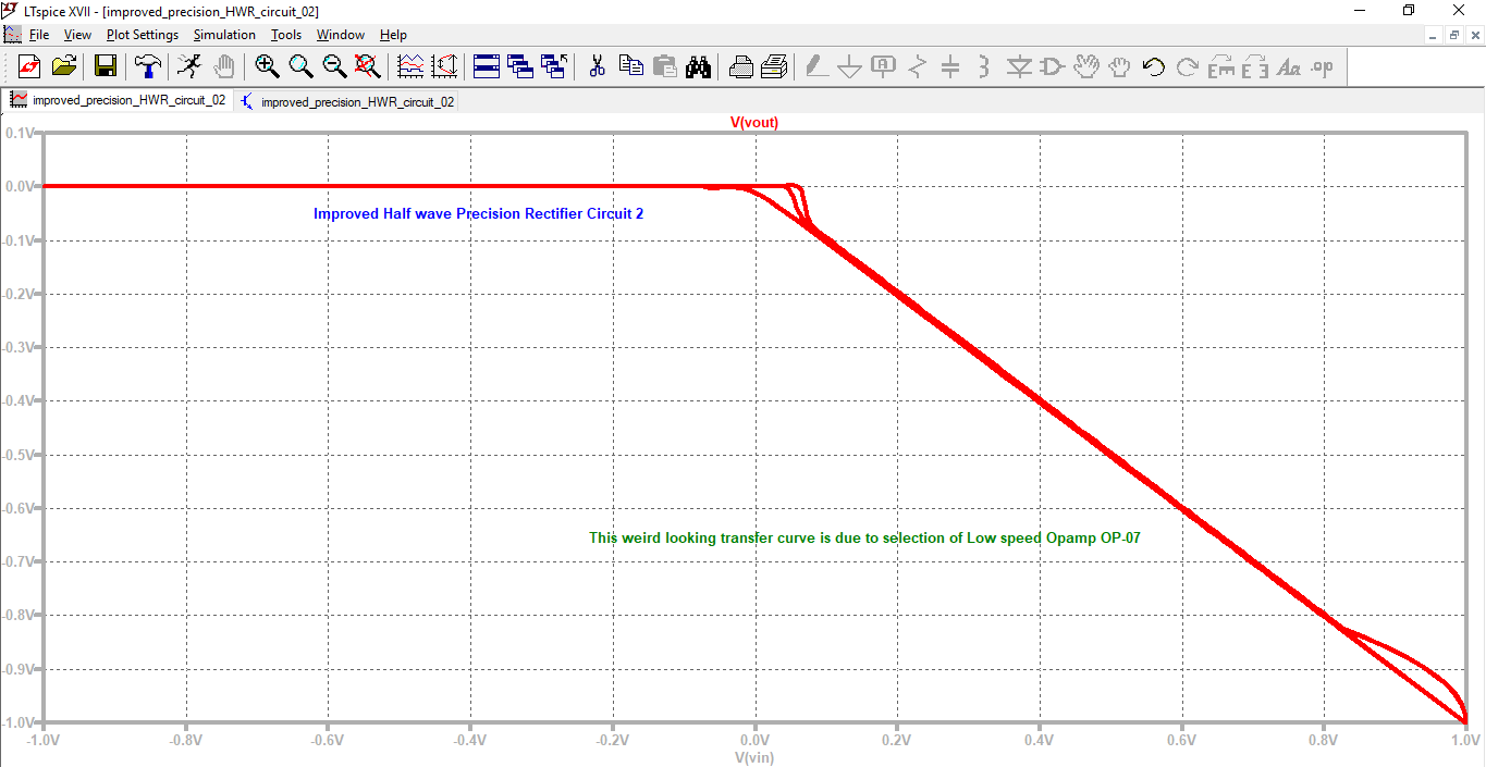
SIMULATION 17.06: Transfer curve for Improved Precision Half wave rectifier circuit 1
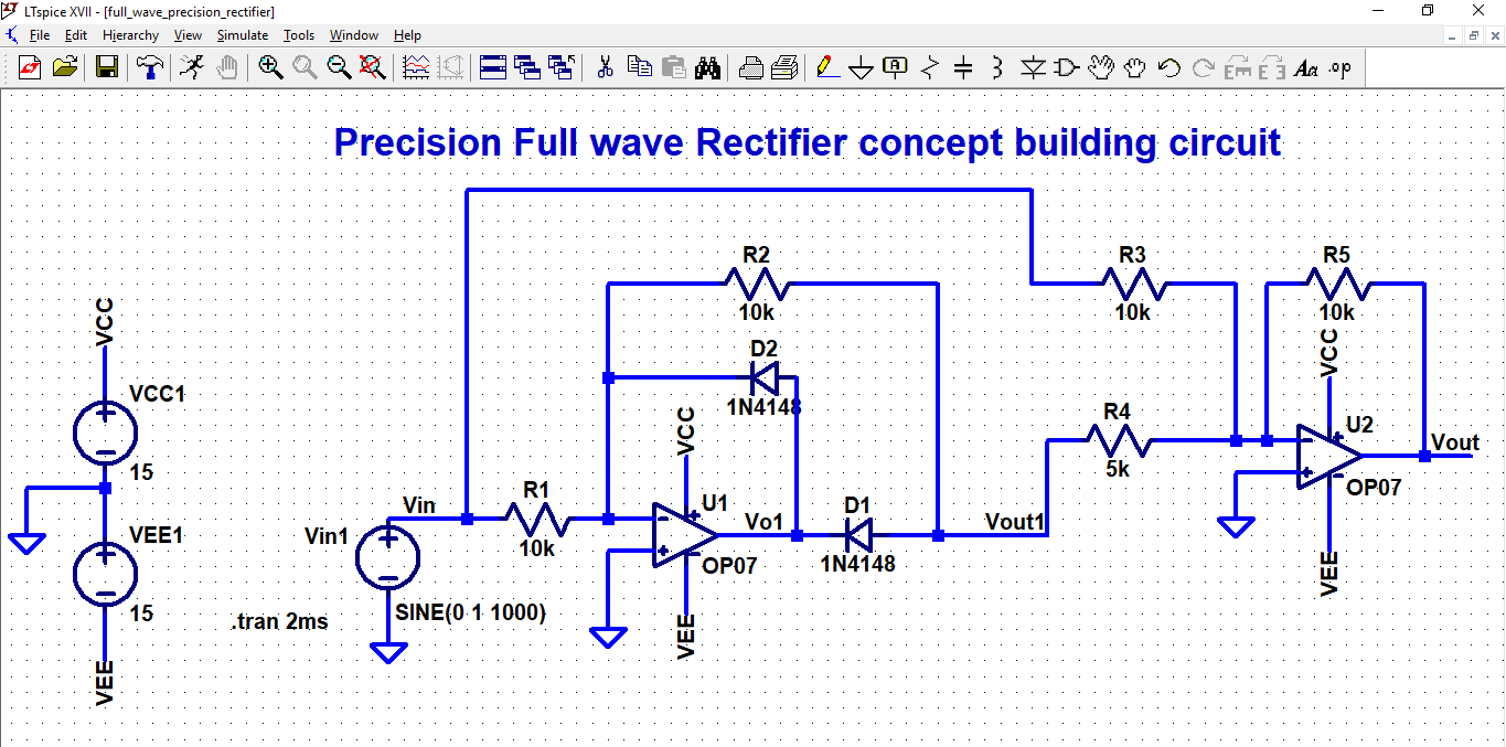
SIMULATION 17.07: Precision Full wave rectifier circuit using Half wave precision circuit+ inverting summer
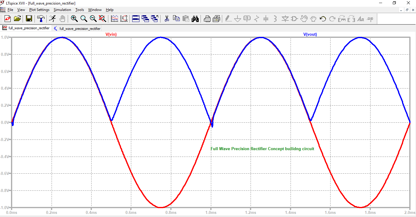
SIMULATION 17.08: Input- output waveform's for Precision Full wave rectifier circuit
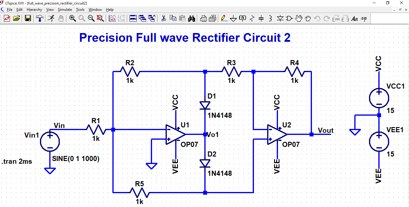
SIMULATION 17.09: Precision Full wave rectifier circuit 2...... This was not simulated in Class..... but one is free to try it out in LT Spice.....
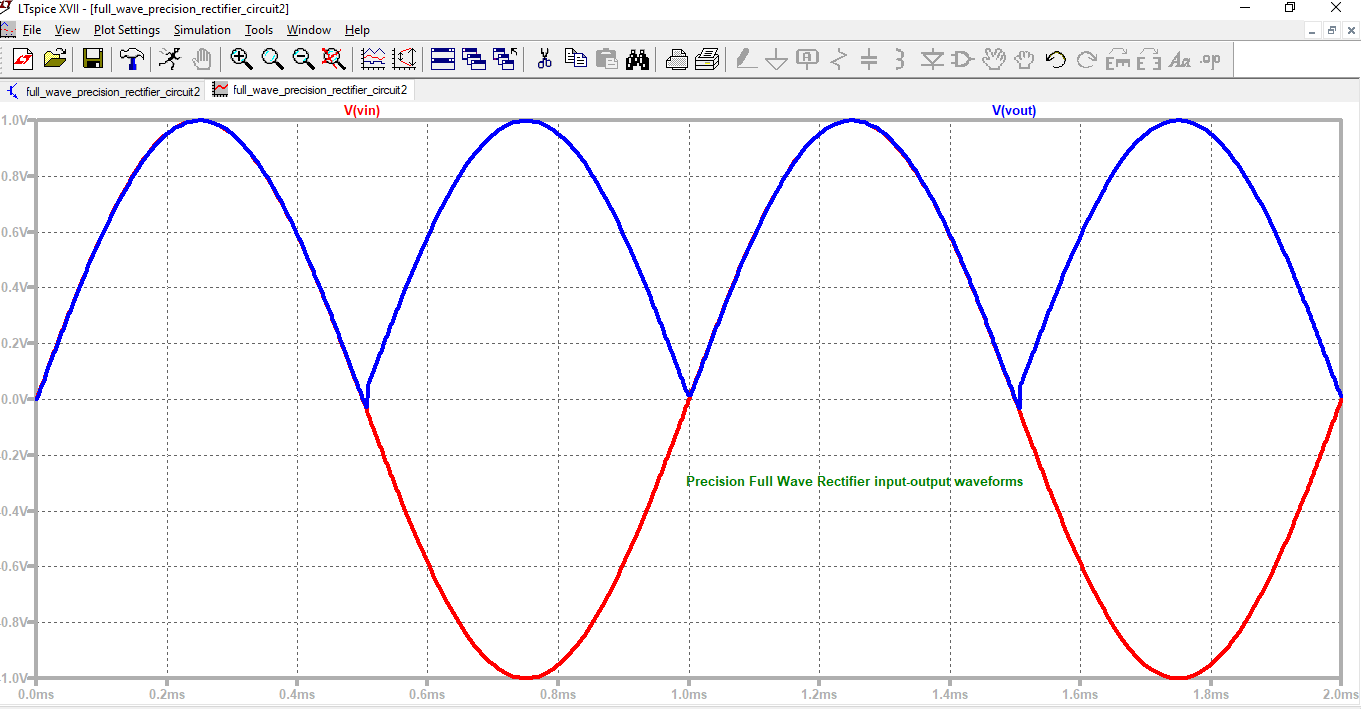
SIMULATION 17.10: Input-Output waveform's for Precision Full wave rectifier circuit 2
Announcement:
There will be NO LICD Weekly Test this week
There will be NO LICD Weekly Test this week
End of Week 05: 14-08-2018 to 16-08-2018
Total no. of Lectures conducted: 02
Total Hours: 02
Activities during week 05:
1) Concepts: Demonstrated in LT Spice schematic and simulation tool
2) Numerical examples: Demonstrated in LT Spice schematic and simulation tool
3) Use of LIVE Quiz in class
4) WHY, HOW and WHERE approach (for circuits) was adopted in Live class
5) Use of Analogy examples to explain difficult topics
Lecture 18 handout dated 21-08-2018
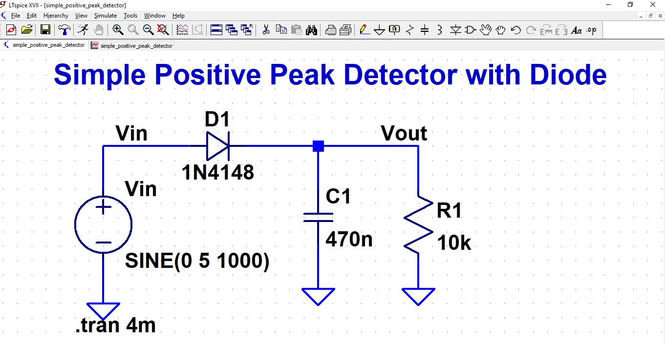
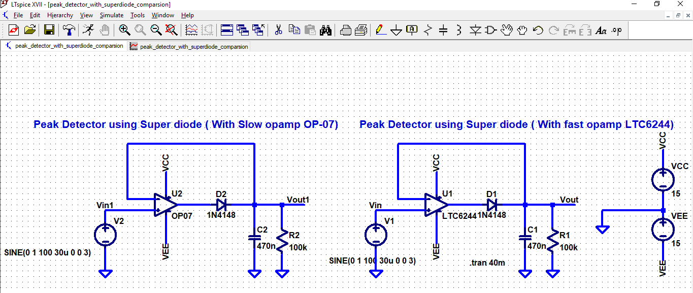
Topics Covered: Simple positive peak detector using diode and limitations associated with it, Peak detector with super diode (Precision peak detector) and limitations associated with it, Peak detector with super diode with buffer (Precision peak detector) and limitations associated with it, Active Peak Detector circuit, Simulation results were demonstrated of all the above circuits and discussed live in class.
Topics Covered: Simple positive peak detector using diode and limitations associated with it, Peak detector with super diode (Precision peak detector) and limitations associated with it, Peak detector with super diode with buffer (Precision peak detector) and limitations associated with it, Active Peak Detector circuit, Simulation results were demonstrated of all the above circuits and discussed live in class.
| licd_18.pdf |
SIMULATIONS related to lecture 18 are below : 18.01 to 18.10 ( Total 10 images)
SIMULATION 18.01: Simple Positive Peak Detector circuit using Diodes
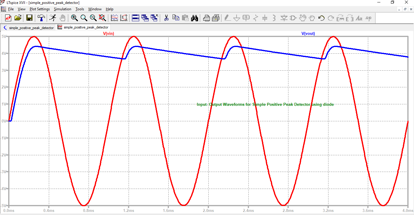
SIMULATION 18.02: Input- Output Wave-forms of Simple Positive Peak Detector circuit using Diodes
Limitations:
1) Output is short of peak by one diode drop (0.7V)
2) Input resistance is changing due to non-linear characteristics of diode.
3) Discharging rate is limited by R1 and C1, as a result output voltage drops a little until it reaches input again as evident from waveform below
Limitations:
1) Output is short of peak by one diode drop (0.7V)
2) Input resistance is changing due to non-linear characteristics of diode.
3) Discharging rate is limited by R1 and C1, as a result output voltage drops a little until it reaches input again as evident from waveform below
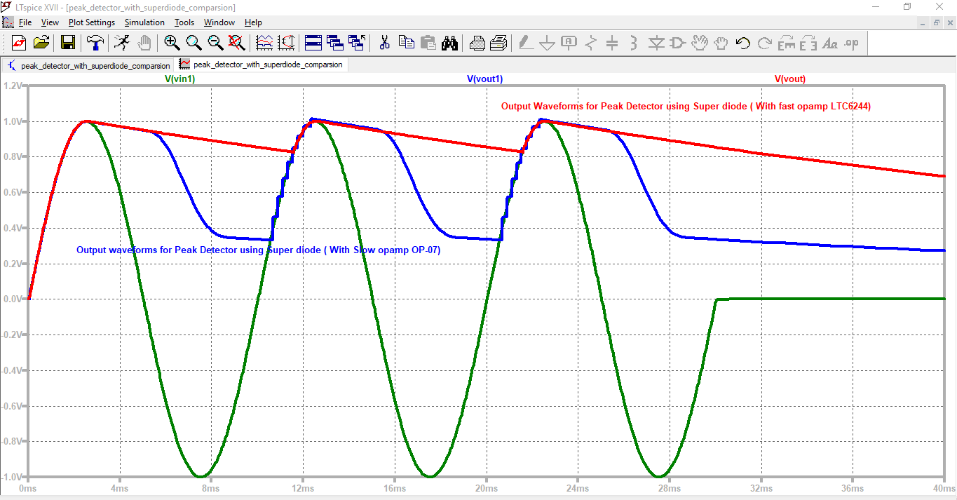
SIMULATION 18.03: Positive Peak Detector circuit using Super Diodes
Two Circuits are simulated below: One is with slower opamp(OP-07) and faster opamp(LTC6244)
Two Circuits are simulated below: One is with slower opamp(OP-07) and faster opamp(LTC6244)
SIMULATION 18.04: Input- Output Wave-forms of Positive Peak Detector circuit using Super Diodes ( Two Circuits Performing like one as Fiat Car(slow, sluggish output) and Other as Ferrari Car(Fast,clean output)
Limitations:
1) Discharging rate is limited by R1 and C1, as a result output voltage drops a little until it reaches input again as evident from waveform below
2) Performance of Peak detector very much depends on OPAMP response as well as evident from waveform below.
3) Output of Opamp goes into negative saturation momentarily, and it takes some time to come out of saturation, this will limit the frequency at which circuit can operate.
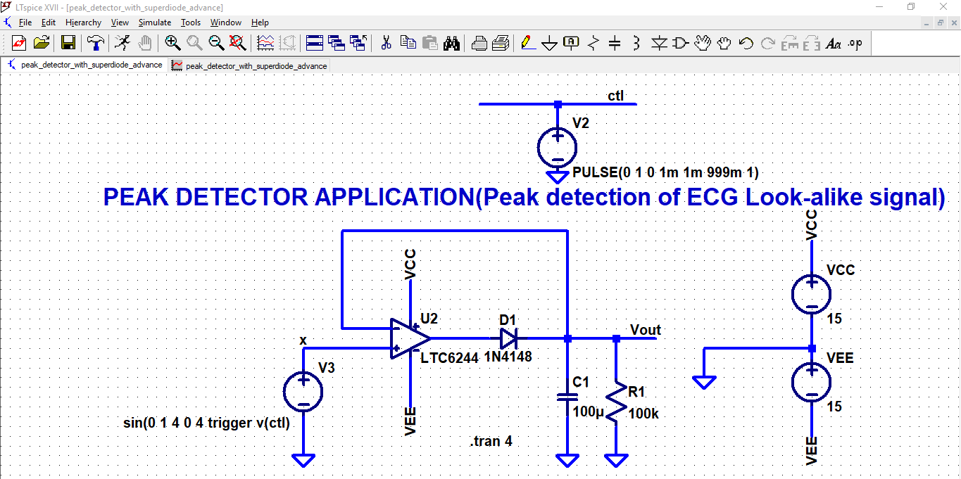
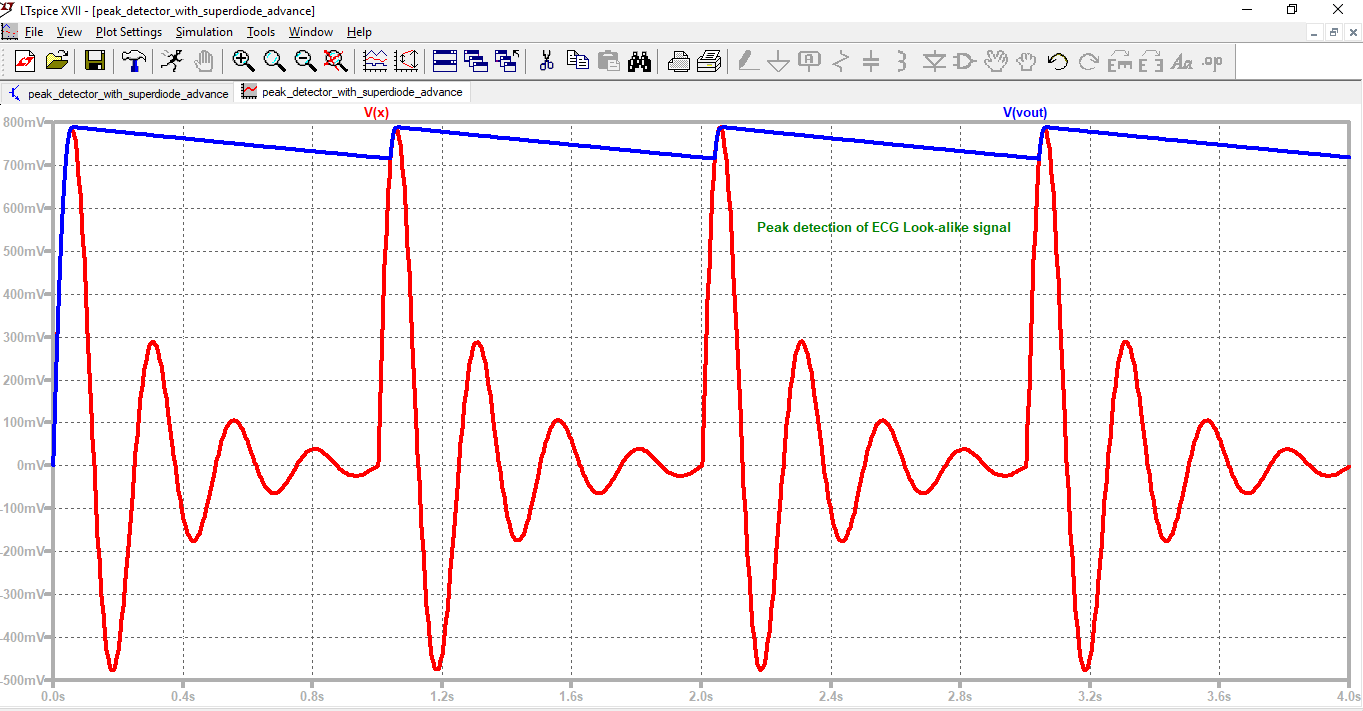
SIMULATION 18.05: Peak Detector application (Peak detection of ECG Look-alike signal)
SIMULATION 18.06: Input- Output Wave-forms of Positive Peak Detector application (Peak detection of ECG Look-alike signal)
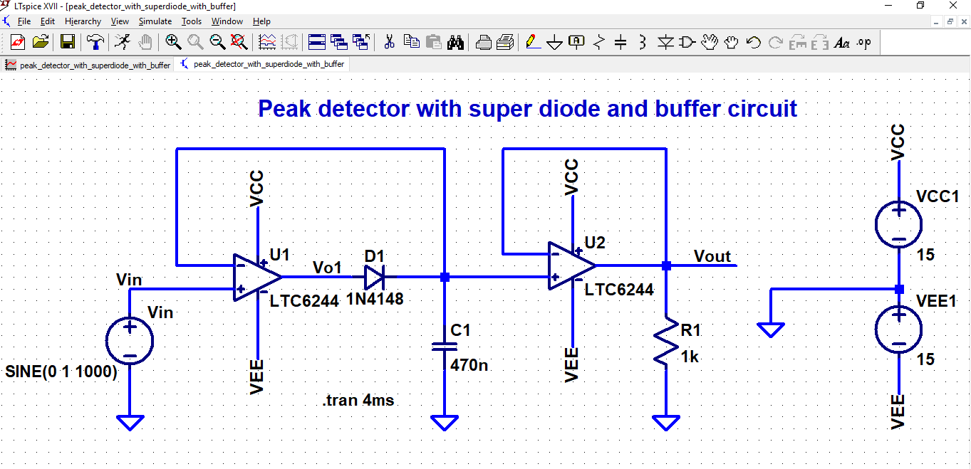
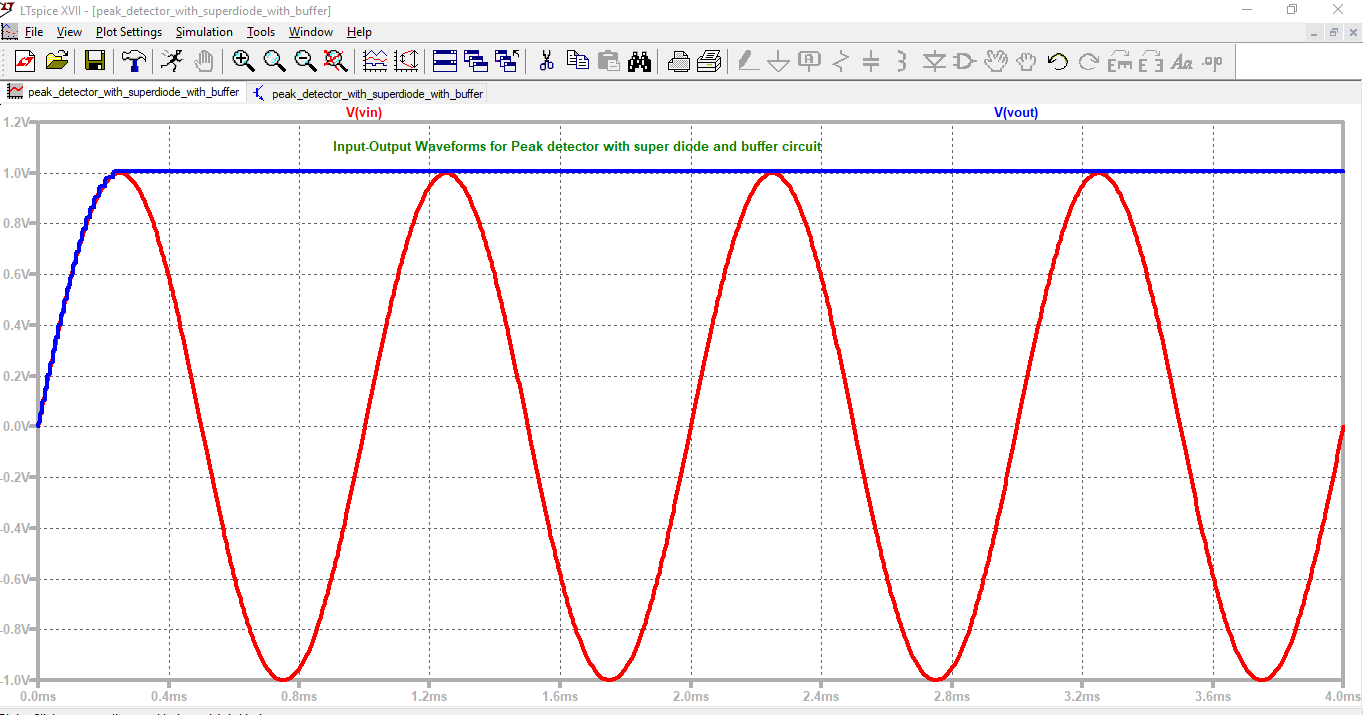
SIMULATION 18.07: Positive Peak Detector circuit using Super Diodes and Buffer
SIMULATION 18.08: Input- Output Wave-forms of Positive Peak Detector circuit using Super Diodes and buffer
Limitations:
1) Output of Opamp 1 goes into negative saturation momentarily, and it takes some time to come out of saturation, this will limit the frequency at which circuit can operate.
Limitations:
1) Output of Opamp 1 goes into negative saturation momentarily, and it takes some time to come out of saturation, this will limit the frequency at which circuit can operate.
SIMULATION 18.09: Active Peak Detector circuit
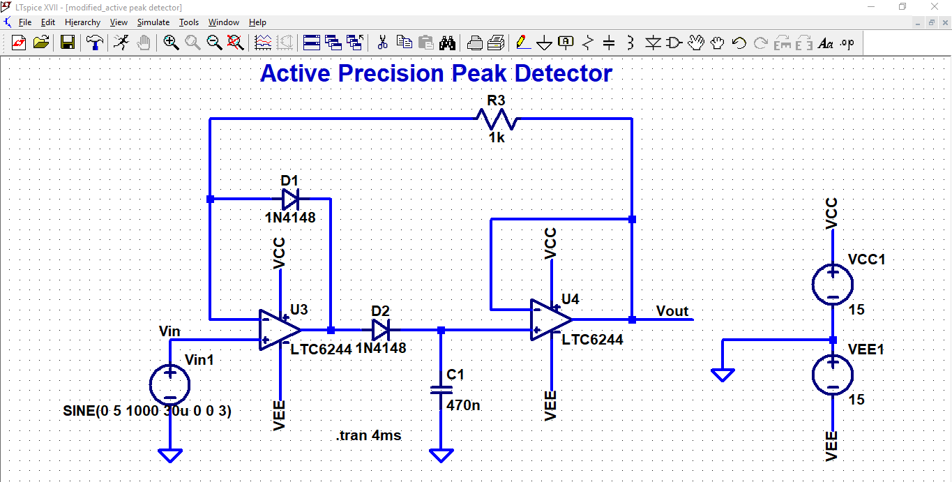
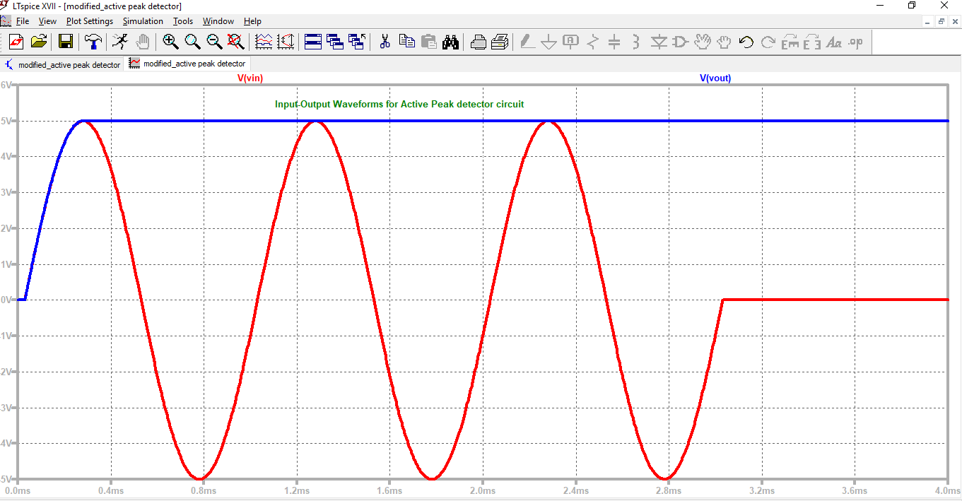
SIMULATION 18.10: Input-Output waveform of Active Peak Detector circuit
-->The output detects the peak of the input signal nicely
Limitations:
1) Voltage drooping and Sagback effect ( to be discussed later)
-->The output detects the peak of the input signal nicely
Limitations:
1) Voltage drooping and Sagback effect ( to be discussed later)
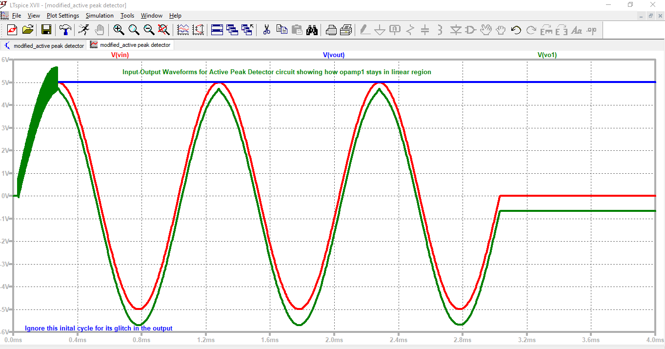
SIMULATION 18.11: Input-Output waveform of Active Peak Detector circuit
-->The output detects the peak of the input signal nicely and also it makes sure that op-amp 1 does not go in to saturation.
Limitations:
1) Voltage drooping and Sagback effect ( to be discussed later)
-->The output detects the peak of the input signal nicely and also it makes sure that op-amp 1 does not go in to saturation.
Limitations:
1) Voltage drooping and Sagback effect ( to be discussed later)
Lecture 19 handout dated 23-08-2018
Topics Covered: Sample and Hold circuit usage (in conversion of Analog(continuous) to discrete signal), Sample and Hold (S/H) circuit operation and waveform, Simulation results were demonstrated (S/H circuit) and discussed live in class, Performance parameters (Acquition time and voltage drooping) of S/H circuit were also discussed in class via simulations.
Topics Covered: Sample and Hold circuit usage (in conversion of Analog(continuous) to discrete signal), Sample and Hold (S/H) circuit operation and waveform, Simulation results were demonstrated (S/H circuit) and discussed live in class, Performance parameters (Acquition time and voltage drooping) of S/H circuit were also discussed in class via simulations.
| licd_19.pdf |
SIMULATIONS related to lecture 19 are below : 19.01 to 19.05 ( Total 05 images)
SIMULATIONS related to lecture 19 are below : 19.01 to 19.05 ( Total 05 images)
SIMULATION 19.01: Sample and Hold (S/H) Circuit
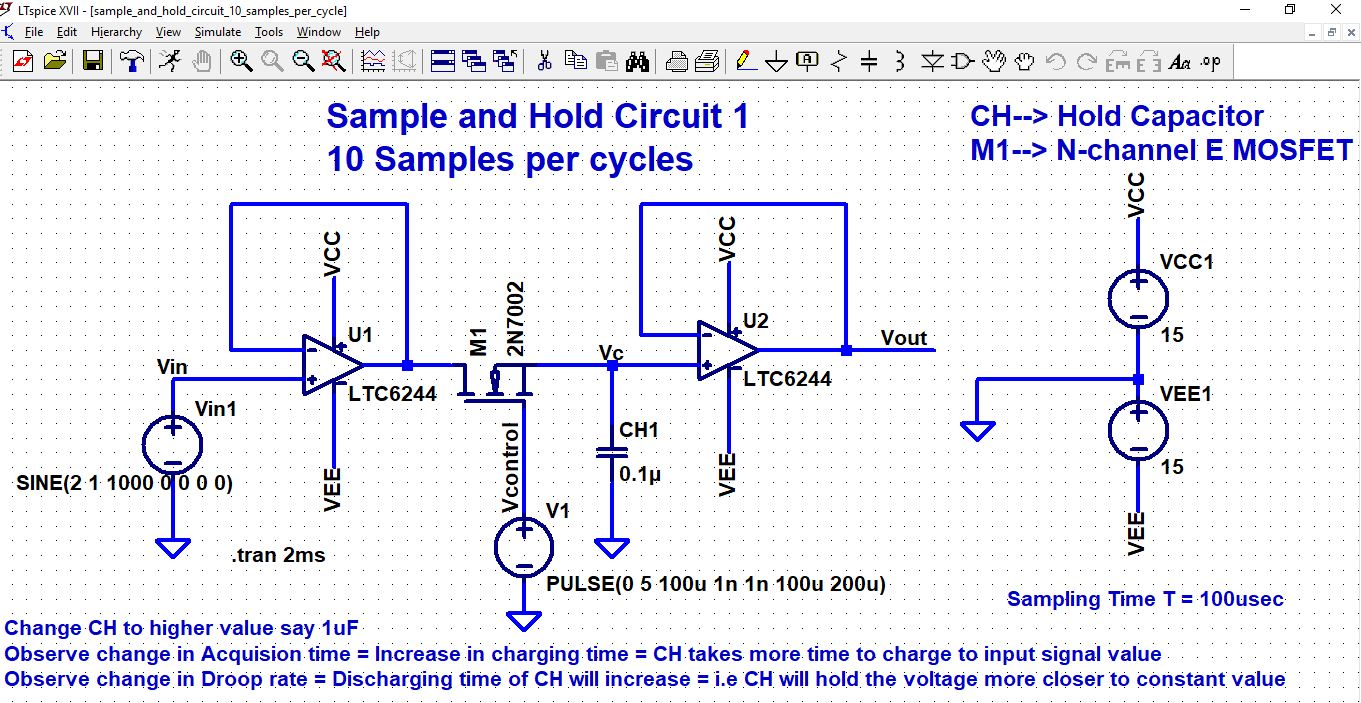
SIMULATION 19.02: Input- Output and Control signal Waveform for (S/H) Circuit with 10 Samples/cycle
SIMULATION 19.03: Input- Output and Control signal Waveform for (S/H) Circuit with 20 Samples/cycle
SIMULATION 19.04: Expanded view of Input- Output and Control signal Waveform for (S/H) Circuit showing Acquisition time
SIMULATION 19.05: Expanded view of Input- Output and Control signal Waveform for (S/H) Circuit showing Voltage Drooping
Lecture 20 handout dated 24-08-2018
Topics Covered: Revisited Ideal opamp equivalent circuit and revised properties of Ideal Opamp, Practical Opamp (e.g IC 741) equivalent circuit,
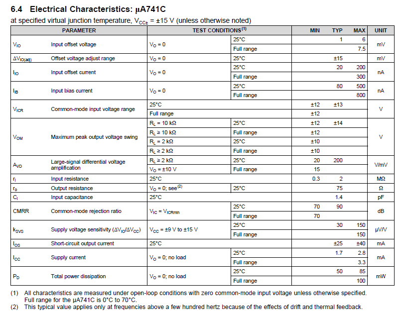
Parameters comparison of Ideal vs 741 opamp, Ideal transfer curve of opamp in open loop configuration, Practical tranfer curve of Opamp in open loop configuration, Necessity of Reducing the open loop gain with negative feedback, CLosed loop Transfer curve for non-inverting amplifier using opamp, Simulation results were demonstrated (741 in open and closed loop mode) and discussed live in class, Analysis of Data sheet uA741C, few electrical parameters ( around 6) were discussed in class.
| licd_20.pdf |
NOTE: In class, LICD midterm 1 syllabus is not been covered yet as of 25-8-18 ...... The design of Practical Integrator and Differentiator circuit is pending.....
SIMULATIONS related to lecture 20 are below : 20.01 to 20.08 ( Total 08 images)
SIMULATION 20.01: OPAMP OP-07 in Open Loop configuration
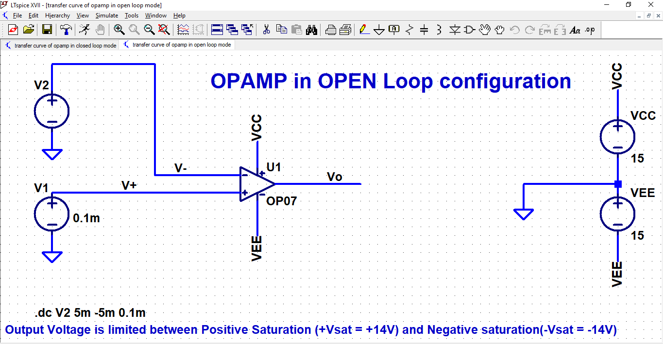
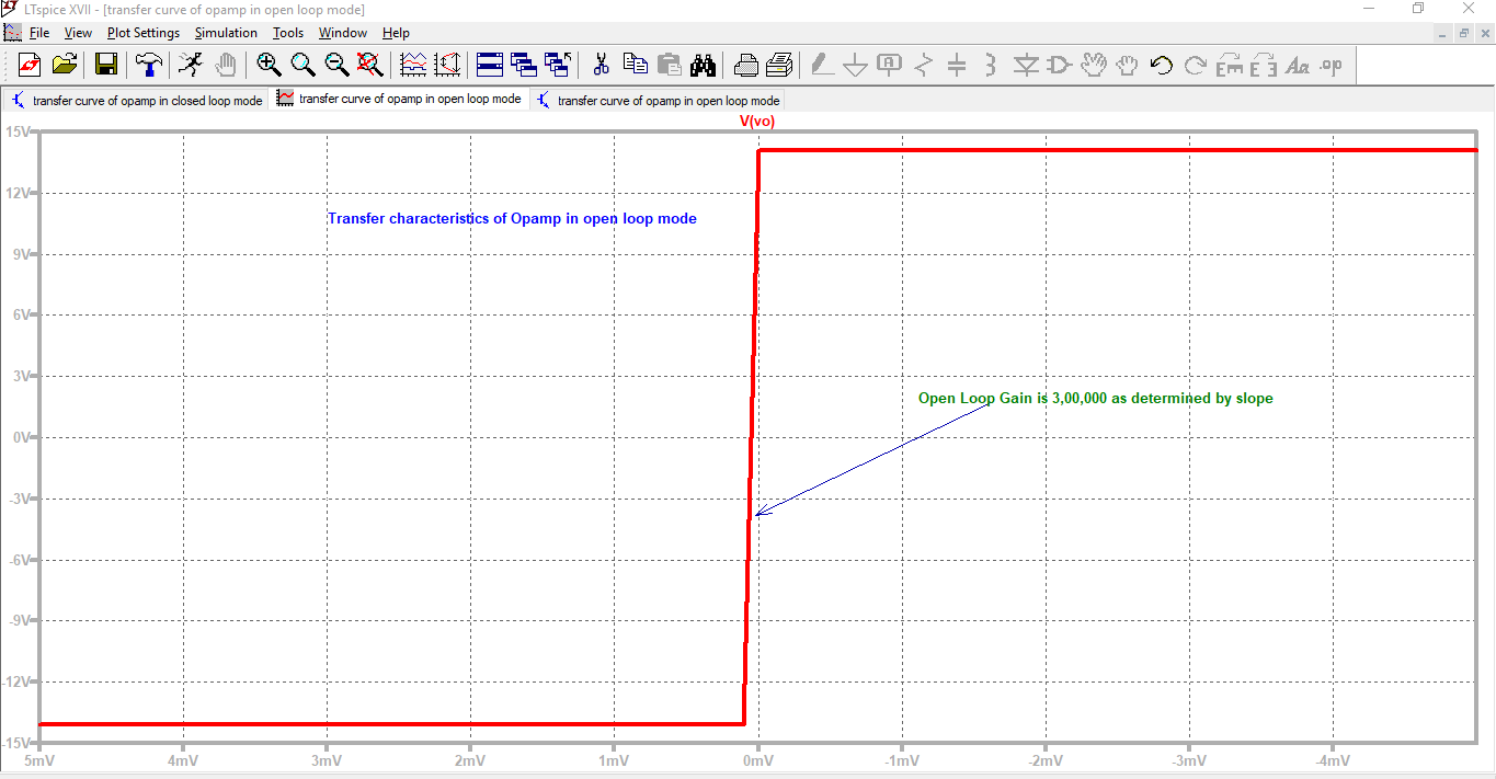
SIMULATION 20.02: Transfer curve of OPAMP OP-07 in Open Loop configuration
The open loop gain is very high gain
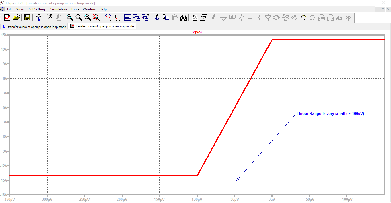
SIMULATION 20.03: Expanded view of Transfer curve of OPAMP OP-07 in Open Loop configuration
As the open loop gain is very high gain, the linear range is very small in micro-volts.
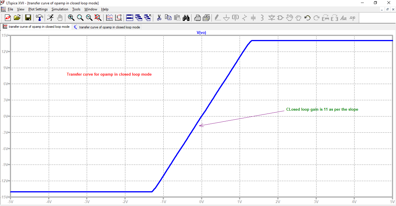
SIMULATION 20.04: Transfer curve of OPAMP OP-07 in Closed Loop configuration
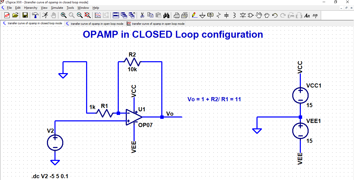
SIMULATION 20.05: Transfer curve of OPAMP OP-07 in Closed Loop configuration
The closed loop gain is 11 as per slope in the curve
The closed loop gain is 11 as per slope in the curve
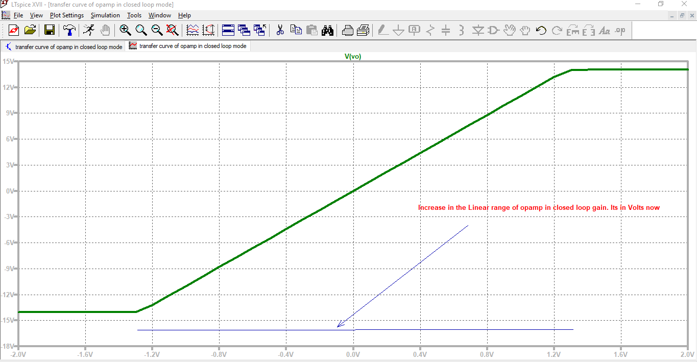
SIMULATION 20.06: Expanded view of Transfer curve of OPAMP OP-07 in CLosed Loop configuration
As the open loop gain is 11(low), the linear range is wide in few volts.
As the open loop gain is 11(low), the linear range is wide in few volts.
SIMULATION 20.07: Typical information available in a DataSheet
Announcement:
NO LICD Weekly Test conducted this week
NO LICD Weekly Test conducted this week
End of Week 06: 21-08-2018 to 24-08-2018
Total no. of Lectures conducted: 03
Total Hours: 03
Activities during week 06:
1) Concepts: Demonstrated in LT Spice schematic and simulation tool
2) Use of LIVE Quiz in class
3) WHY, HOW and WHERE approach (for circuits) was adopted in Live class
4) Use of Analogy examples to explain difficult topics
5) Analysis of a Datasheet
Lecture 21 handout dated 28-08-2018
Topics Covered: Analysis of Data sheet uA741C: Few electrical parameters ( around 6) which were left were discussed in class. Effect of DC offset voltage on non-inverting, inverting amplifier, and integrator circuit. Effect of bias current on non-inverting amplifier, Problems with Ideal integrator w.r.t dc offset and remedial technique to make a improved integrator.
Even though, students (total:05) were less in number, still conducted since we have to reach till design of Practical Integrator and Practical differentiator for completion of Term test 1 syllabus.
| licd_21.pdf |
Video related to lecture 21 is below : 21.01 to 21.02 ( Total 2 )
Video 21.01 : Excellent lecture on Opamp Non-idealities
Video 21.02a : IITB Professor lecture on Opamp Non-idealities
Video 21.02b : IITB Professor lecture on Opamp Non-idealities
Make-up Lecture 02 handout (To cover up for lecture dated 29-08-2018)
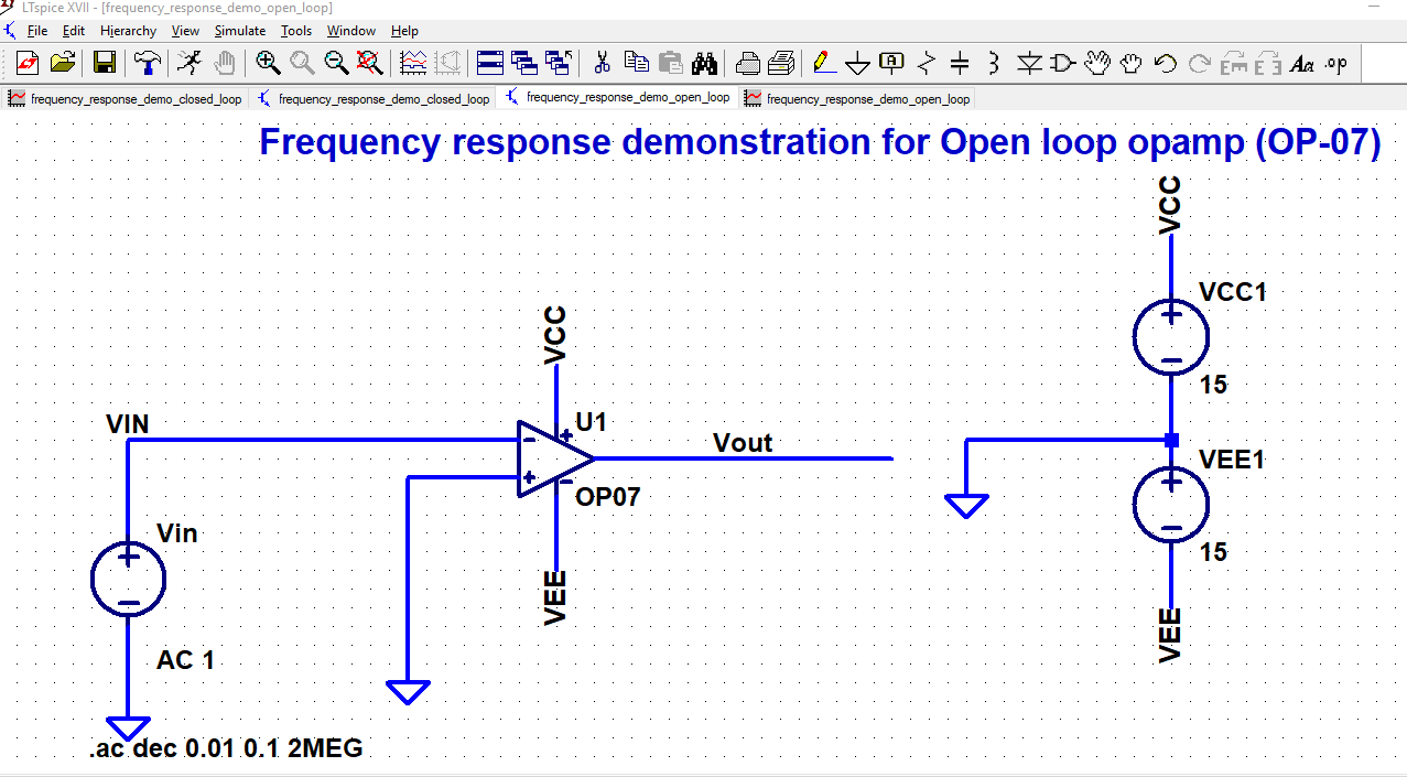
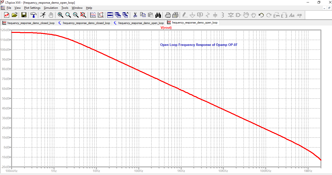
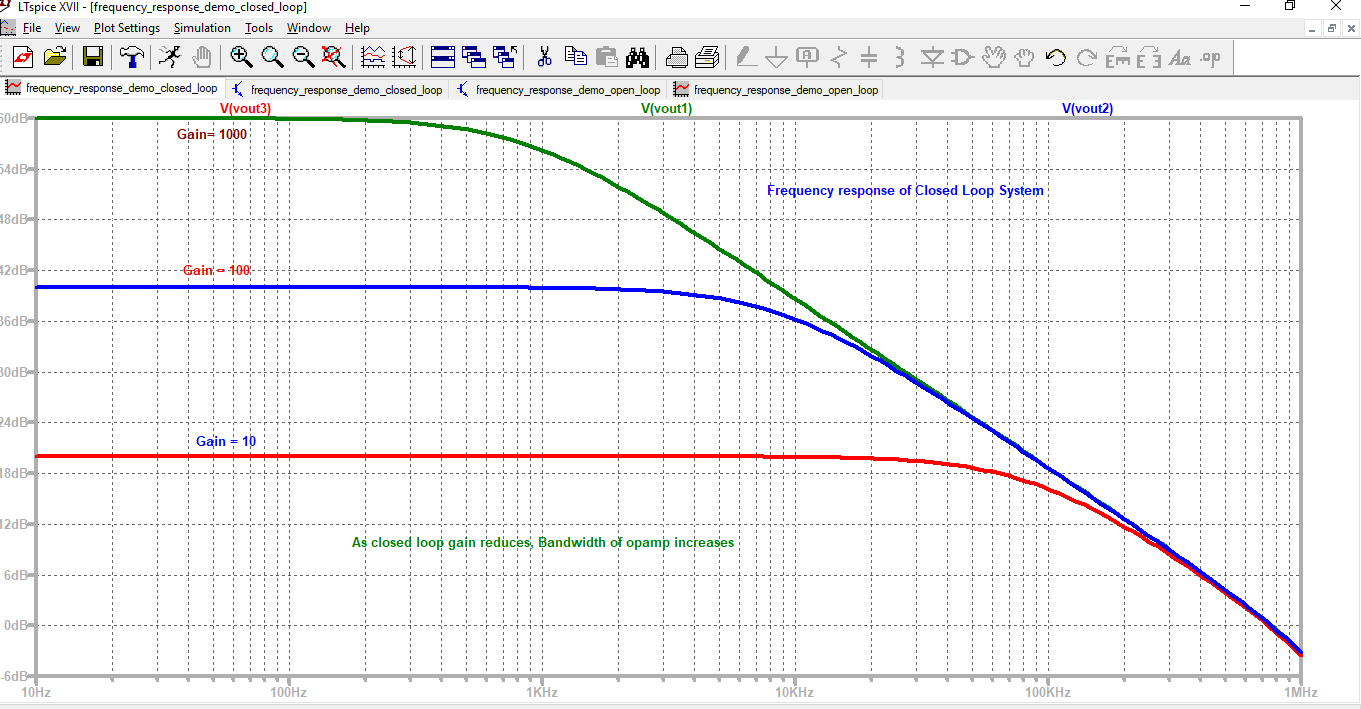
Topics Covered: Frequency response of opamp in open loop configuration and demonstration of the same in LT Spice, Frequency response of opamp in closed loop configuration and demonstration of the same in LT Spice
Topics Covered: Frequency response of opamp in open loop configuration and demonstration of the same in LT Spice, Frequency response of opamp in closed loop configuration and demonstration of the same in LT Spice
| licd_make-up_lecture_02.pdf |
SIMULATIONS related to make-up lecture 02 are below : 02.01 to 02.04 ( Total 04 images)
SIMULATION 02.01: Open loop op-amp circuit configuration for analyzing it's frequency response
SIMULATION 02.02 : Open loop frequency response for Opamp
SIMULATION 02.03 : Inverting amplifier op-amp circuit for analyzing Closed Loop frequency response
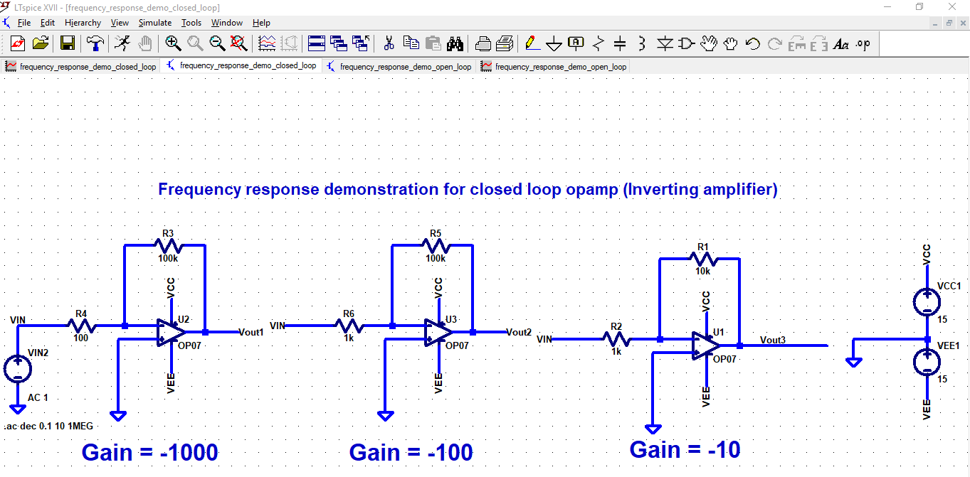
SIMULATION 02.04 : Comparison of various closed loop gains in case of Closed Loop frequency response
Make-up Lecture 03 handout (To cover up for lecture dated 30-08-2018)
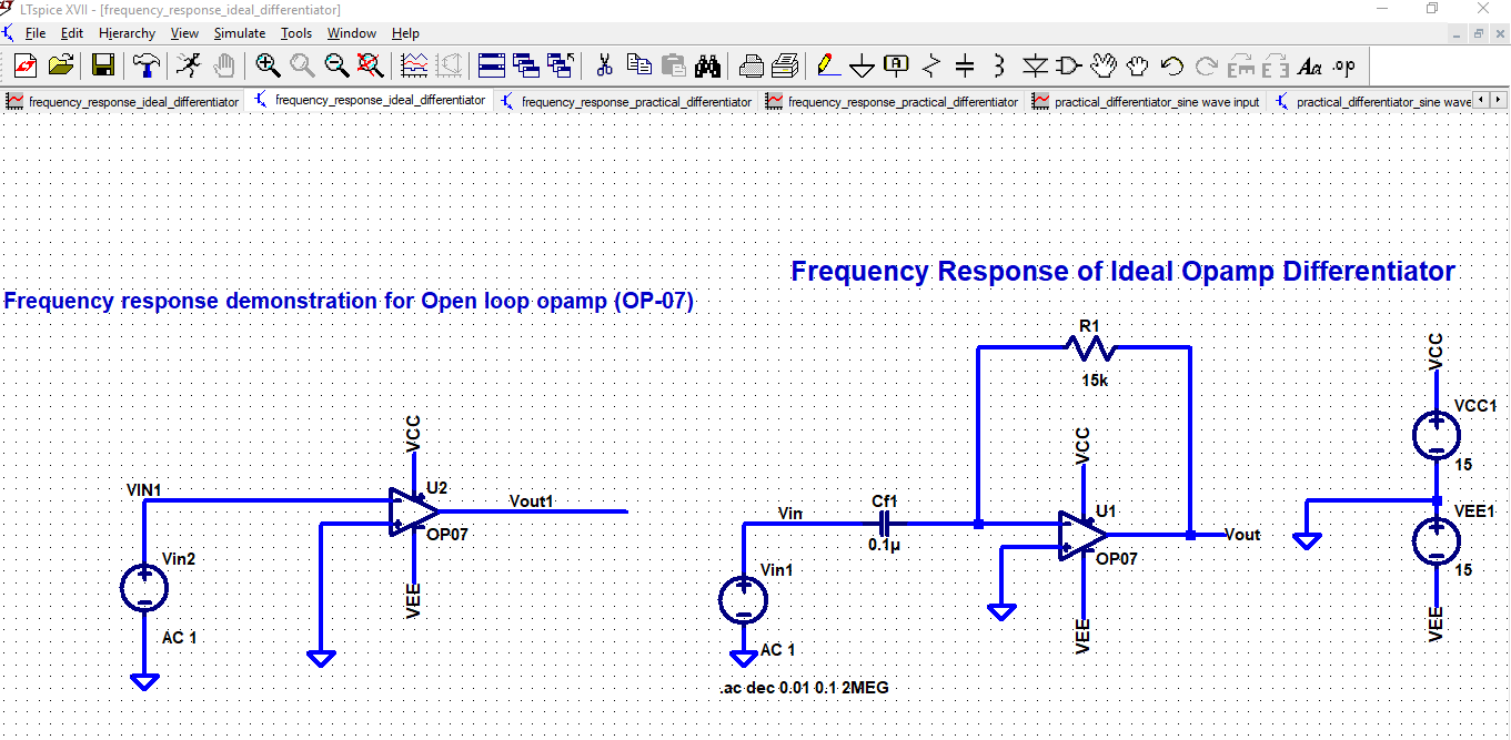
Topics Covered: Analysis of Ideal Integrator in frequency domain, frequency response of Ideal Integrator (with demonstration in LT Spice), Problems associated with ideal integrator, Concept building for Practical Integrator, Practical integrator circuit frequency response ((with demonstration in LT Spice), and design of practical integrator circuit using opamp
| licd_make-up_lecture_03.pdf |
SIMULATIONS related to make-up lecture 03 are below : 03.01 to 03.06 ( Total 06 images)
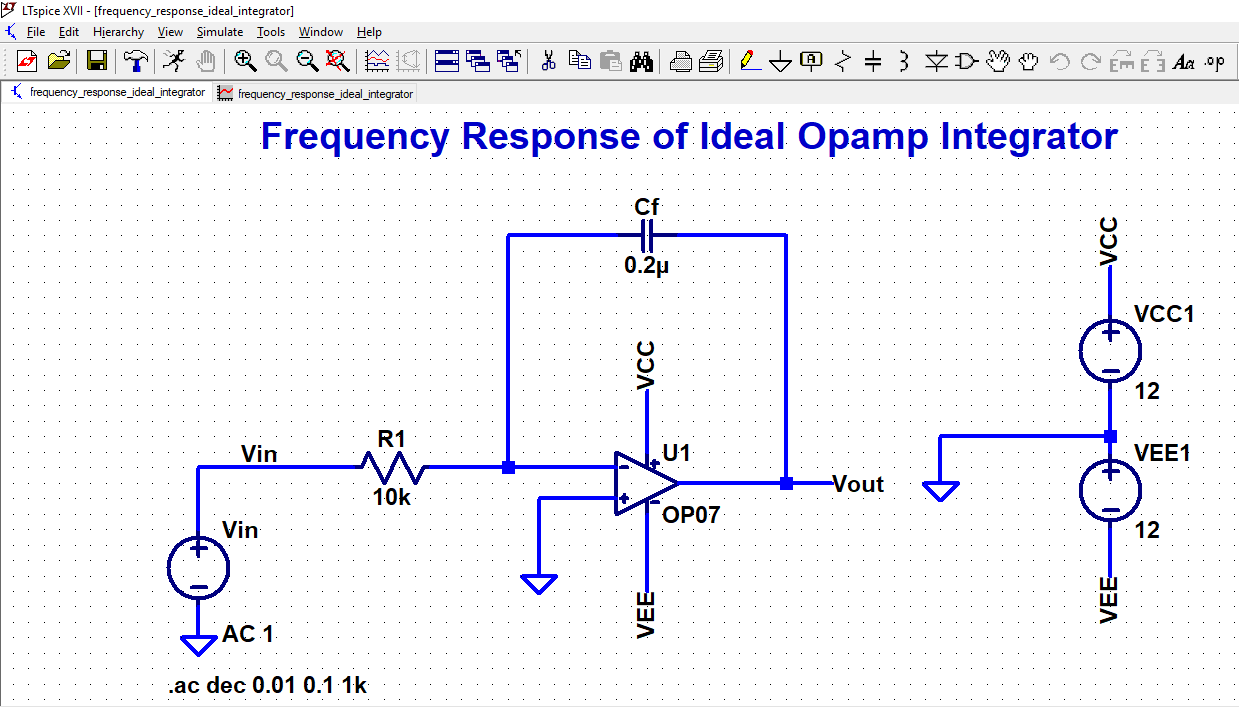
SIMULATION 03.01 : Ideal Integrator Circuit using opamp
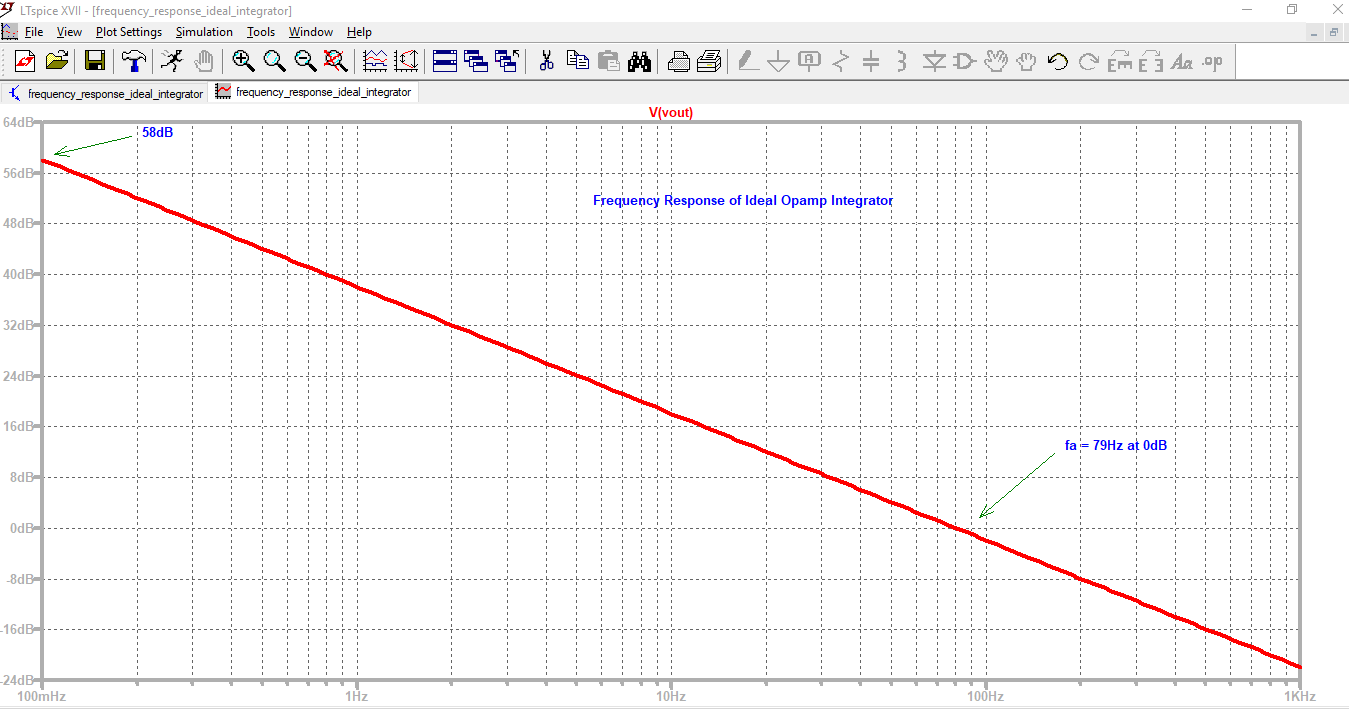
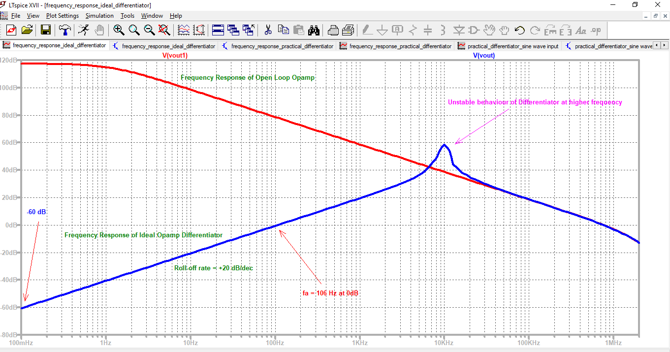
SIMULATION 03.02 : Frequency Response of Ideal Opamp Integrator
SIMULATION 03.03 : Ideal Integrator and Practical Integrator circuits using Opamp
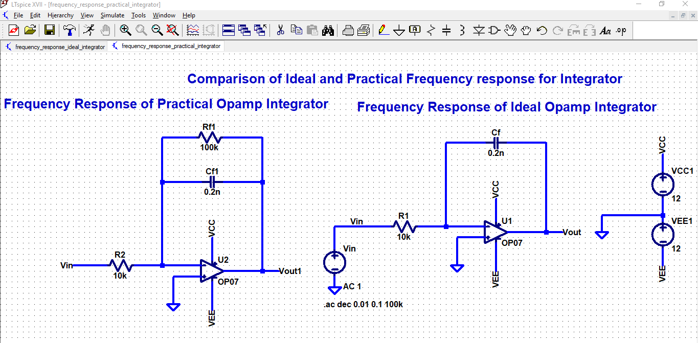
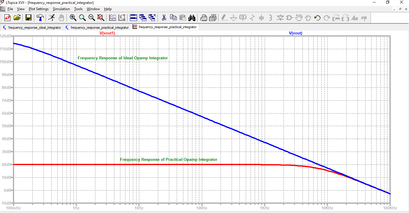
SIMULATION 03.04 : Comparison of frequency response of Ideal and Practical Integrator
SIMULATION 03.05 : Practical Integrator circuit with sine and square input
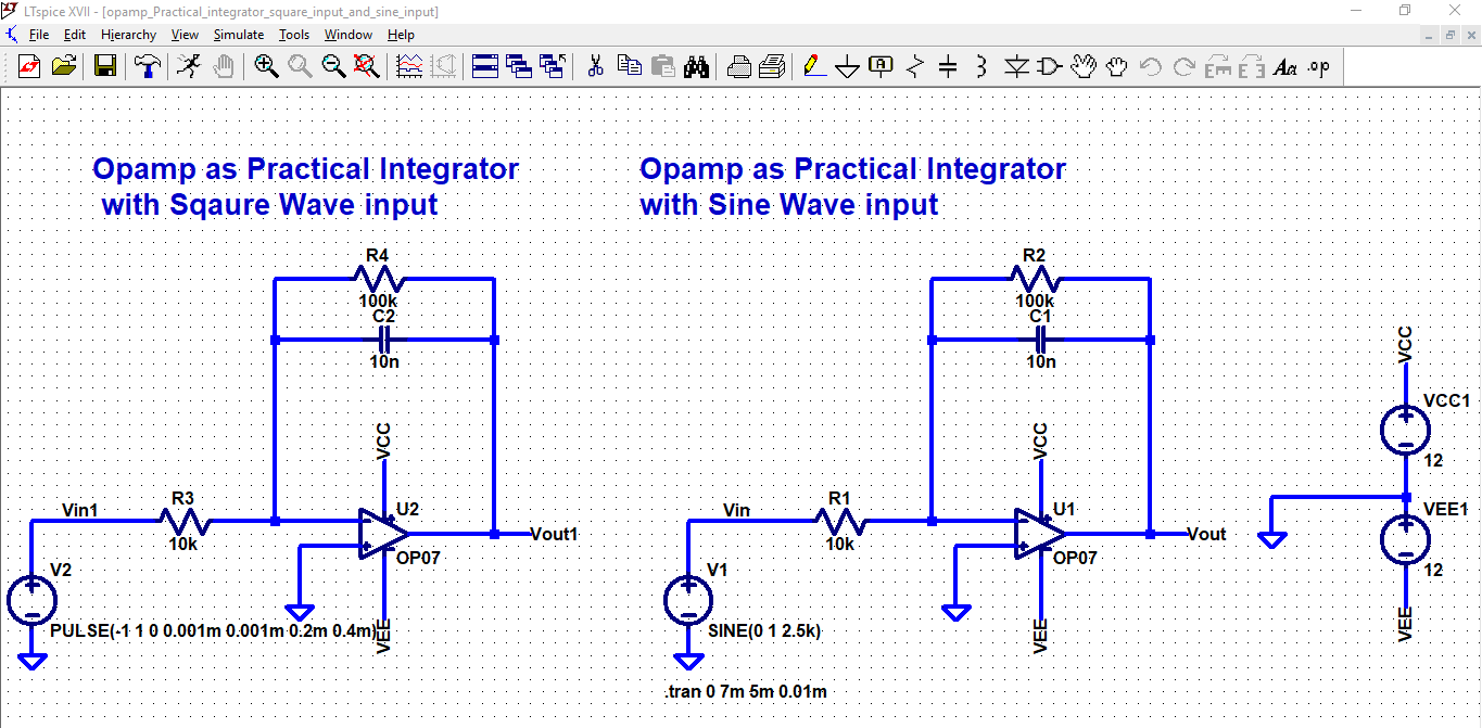
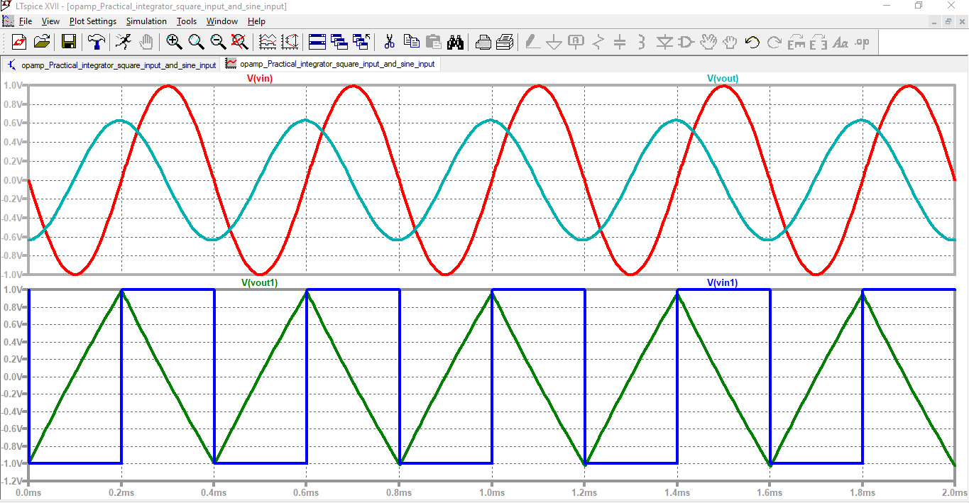
SIMULATION 03.06 : Output of Practical Integrator for sine wave and square inputs
Make-up Lecture 04 handout (To cover up for lecture dated 31-08-2018)
Topics Covered: Analysis of Ideal Differentiator in frequency domain, frequency response of Ideal Differentiator (with demonstration in LT Spice), Problems associated with ideal Differentiator, Concept building for Practical Differentiator, Practical Differentiator circuit frequency response ((with demonstration in LT Spice), and design of practical differentiator circuit using opamp, distinguish between Integrator and Differentiator
| licd_make-up_lecture_04.pdf |
SIMULATIONS related to make-up lecture 04 are below : 04.01 to 04.10 ( Total 10 images)
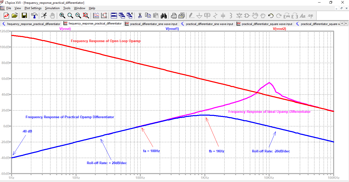
SIMULATION 04.01 : Ideal Opamp Differentiator circuit
SIMULATION 04.02 : Frequency response of Ideal Opamp Differentiator compared with open loop frequency response of opamp
SIMULATION 04.03 : Practical Opamp Differentiator circuit
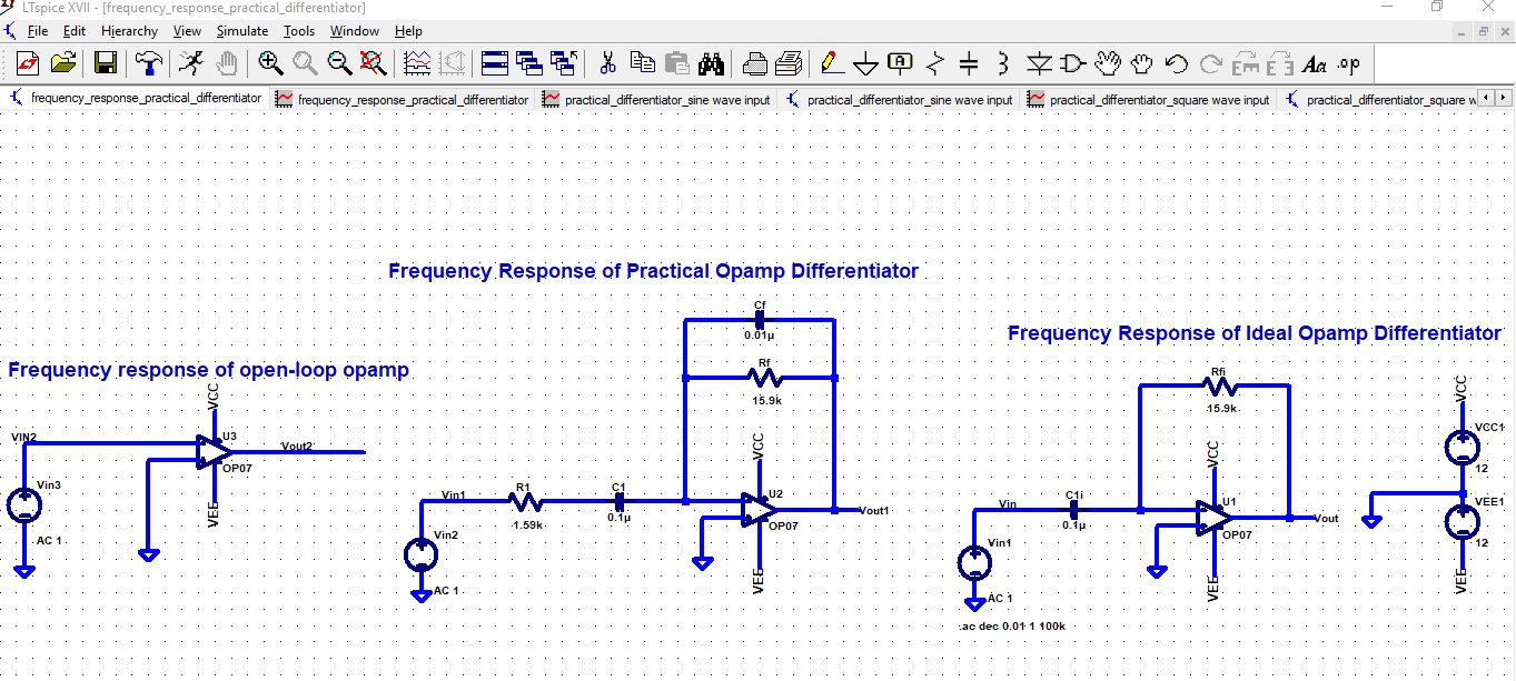
SIMULATION 04.04 : Frequency response of Ideal and Practical Opamp Differentiator compared with open loop frequency response of opamp
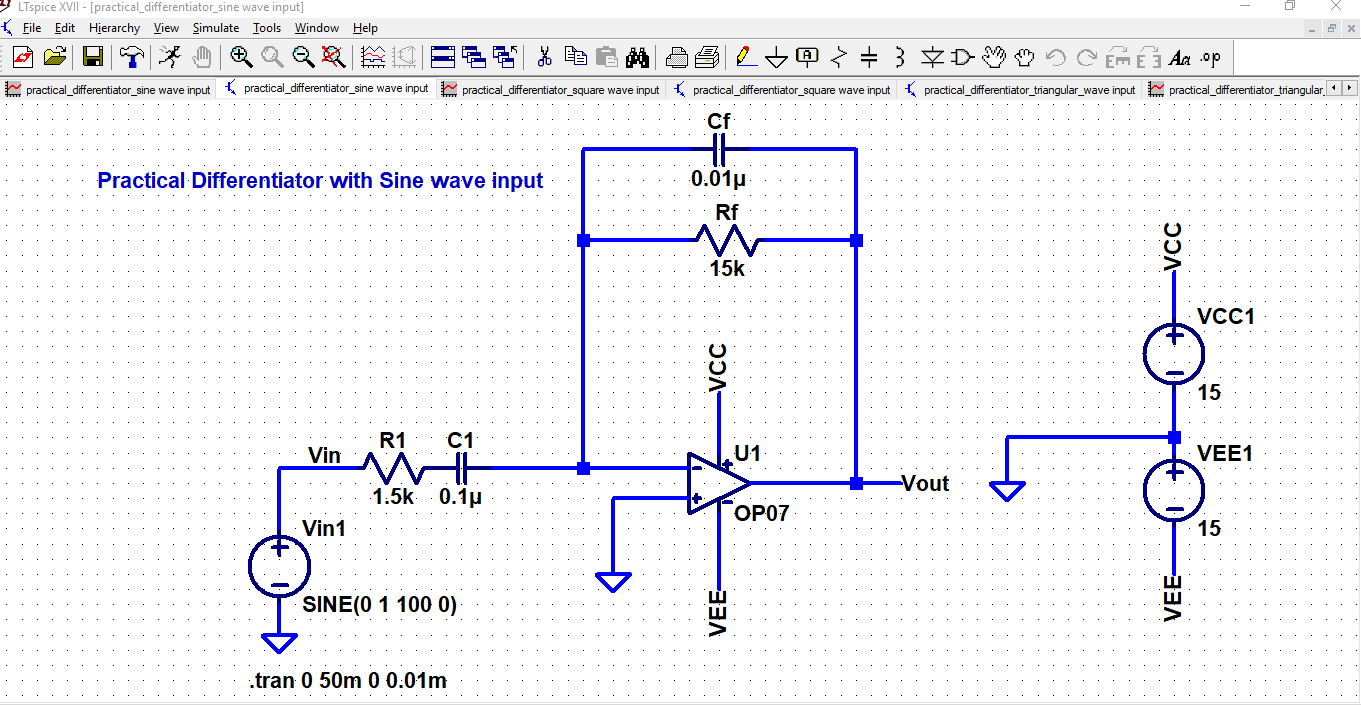
SIMULATION 04.05 : Practical Opamp Differentiator circuit with Sine wave input
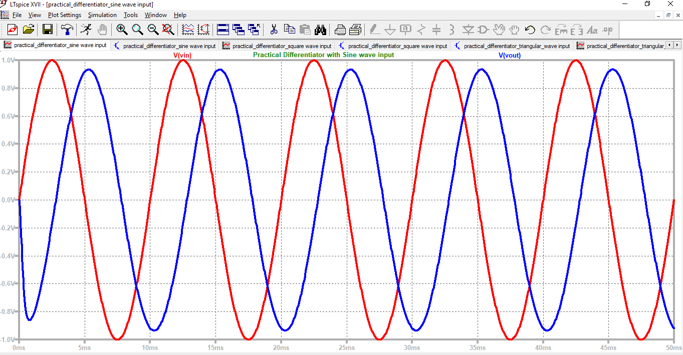
SIMULATION 04.06 : Output of Practical Opamp Differentiator circuit with sine wave input
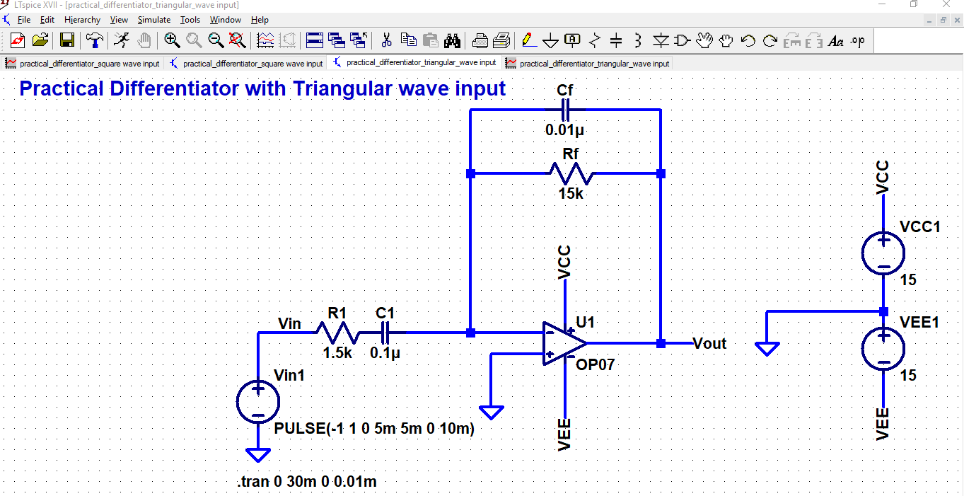
SIMULATION 04.07 : Practical Opamp Differentiator circuit with Triangular wave input
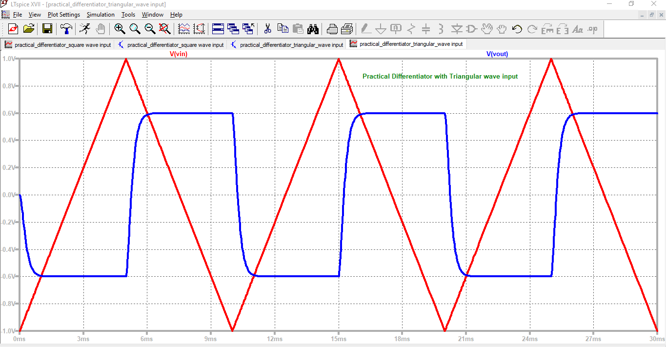
SIMULATION 04.08 : Output of a Practical Opamp Differentiator circuit with Triangular input
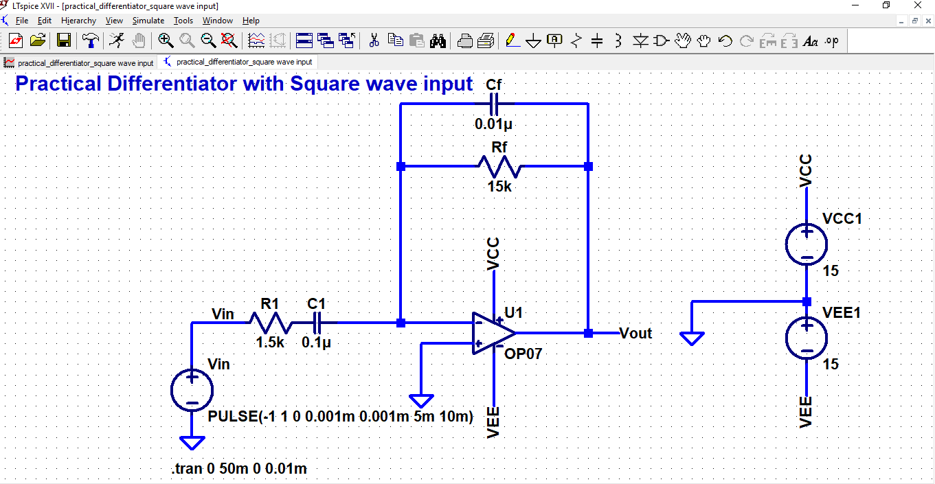
SIMULATION 04.09 : Practical Opamp Differentiator circuit with Square wave input
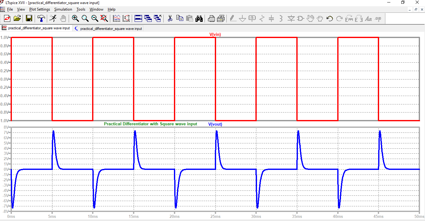
SIMULATION 04.10 : Output of a Practical Opamp Differentiator circuit with Square wave input
Announcement as on 2-9-2018
Regarding Make-up lectures 02,03 and 04 contents
For midterm test 1, one can concentrate on Design of Practical Integrator and Practical differentiator for time being
Make-up lecture contents will be covered in class soon....
Announcement as on 5-9-2018
LICD lecture on 06-09-2018 will be from 10:30 to 11:30 am and then again from 2:15 to 3:15 pm
LICD lecture on 06-09-2018 will be from 10:30 to 11:30 am and then again from 2:15 to 3:15 pm
End of Week 07: 28-08-2018 to 31-08-2018
Total no. of Lectures conducted: 01 ....(barely managed with just 5 students)
Total Hours: 01
Activities during week 07:
1) Concepts taught on green board
Total no. of Lectures conducted: 01 ....(barely managed with just 5 students)
Total Hours: 01
Activities during week 07:
1) Concepts taught on green board
Lecture 22,23 handout dated 06-09-2018: Already uploaded handouts in the form of Make-up Lecture 02 and Make-up lecture 03
Lecture 22
Topics Covered: Frequency response of opamp in open loop configuration and demonstration of the same in LT Spice, Frequency response of opamp in closed loop configuration and demonstration of the same in LT Spice
Lecture 23
Topics Covered: Analysis of Ideal Integrator in frequency domain, frequency response of Ideal Integrator (with demonstration in LT Spice), Problems associated with ideal integrator, Concept building for Practical Integrator, Practical integrator circuit frequency response (with demonstration in LT Spice) and design of practical integrator circuit using opamp
Lecture 24 handout dated 07-09-2018: Already uploaded handouts in the form of Make-up Lecture 04
Topics Covered: Analysis of Ideal Differentiator in frequency domain, frequency response of Ideal Differentiator (with demonstration in LT Spice), Problems associated with ideal Differentiator, Concept building for Practical Differentiator, Practical Differentiator circuit frequency response ((with demonstration in LT Spice), and design of practical differentiator circuit using opamp, distinguish between Integrator and Differentiator
End of Week 08: 04-09-2018 to 07-09-2018
Total no. of Lectures conducted: 03
Total Hours: 03
Activities during week 08:
1) Concepts taught on green board
2) Practical designs topics covered in class for Integrator and Differentiator
3) Simulation plots were demonstration in LT Spice and same were discussed in the class with designs numerical's.
LICD MID TERM TEST 1 Solution
| licd_test_1_solution_september_2018.pdf |
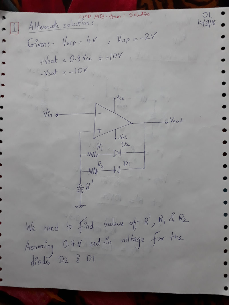
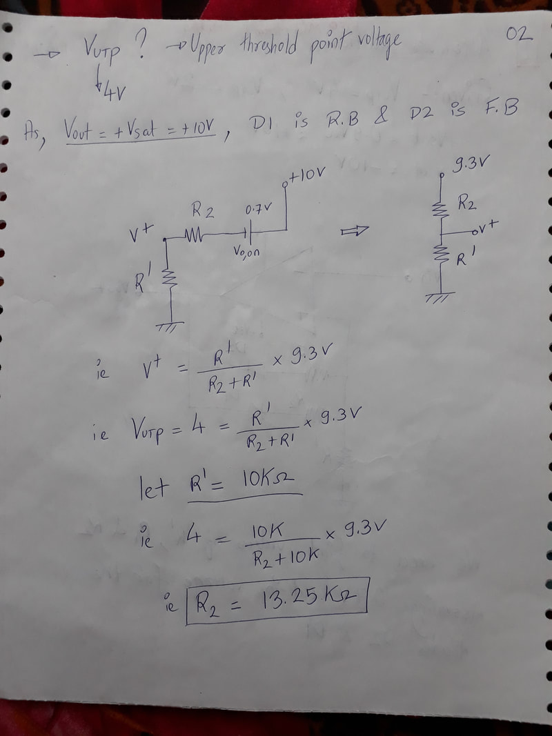
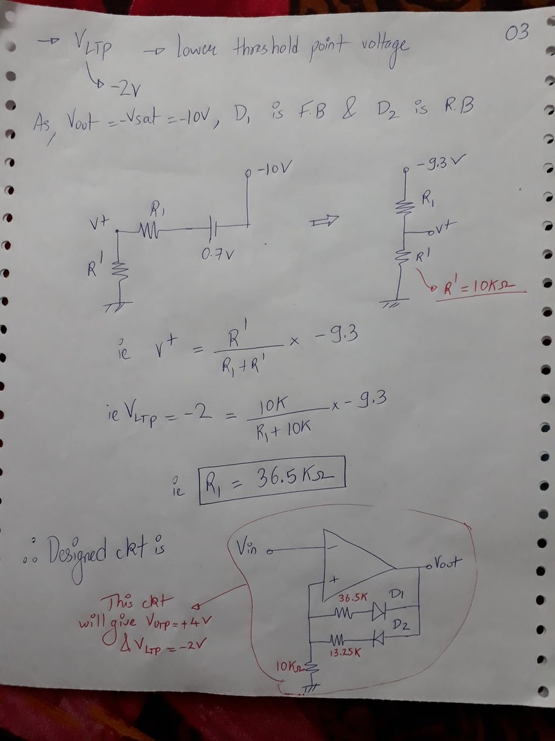
Alternate Solution to Question no 1 is given in 3 images below:
LICD MID TERM 2 Syllabus Starts from Lecture 25 onward's
Lecture 25 handout dated 11-09-2018
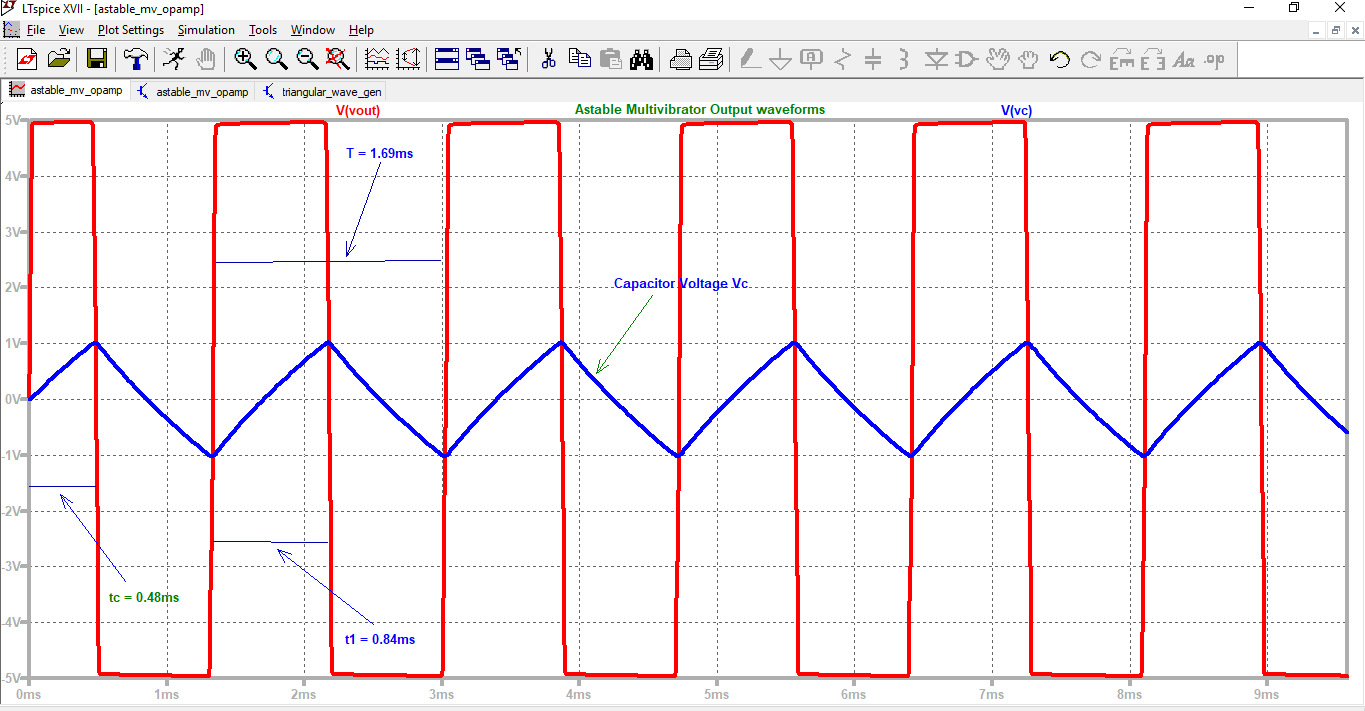
Topics Covered: Concept of Astable with analogy, Revisit Inverting Schmitt trigger, Waveform generation using Schmitt trigger (i.e Astable Multi-vibrator/ Square Wave generator) working with e.g Numerical values, Analysis of waveform along with demonstration in LT Spice
Topics Not covered: Derivation for time period/ frequency of square wave output for an Astable multi-vibrator, Output amplitude limited by back to back zener diode
| licd_25.pdf |
Video related to lecture 25 is below : 25.01 to 25.02 (Total 2)
Video 25.01 : Air piano project (A motivation to study Astable or Square wave generator using opamp)
Description: Simple Air Piano using IR sensor pair and Op-amps. The Relays are acting as switches. Each of the 8 octaves are connected to a single LM741 in astable state, but the resistor combinations are set as per the frequency requirement of the particular note( Sa, Re, Ga, Ma, Pa , Dha, Ni, Sa)
Description: Simple Air Piano using IR sensor pair and Op-amps. The Relays are acting as switches. Each of the 8 octaves are connected to a single LM741 in astable state, but the resistor combinations are set as per the frequency requirement of the particular note( Sa, Re, Ga, Ma, Pa , Dha, Ni, Sa)
Video 25.02 : IITB Professor lecture on Square wave generator/ Astable Multivibrator
One can start video from 10 minutes 05 sec and watch it till 22 minutes 55 sec
One can start video from 10 minutes 05 sec and watch it till 22 minutes 55 sec
Video 25.03 : MIT lecture on Square wave oscillator/ Astable Multi-vibrator Part 1
Video 25.04 : MIT lecture on Square wave oscillator/ Astable Multi-vibrator Part 2
Kindly Note: the syntax used in the video is slightly different than what we used in the class but the concept remains the same
Kindly Note: the syntax used in the video is slightly different than what we used in the class but the concept remains the same
Video 25.05 : MIT lecture on Square wave oscillator/ Astable Multi-vibrator Part 3
Kindly Note: the syntax used in the video is slightly different than what we used in the class but the concept remains the same
Kindly Note: the syntax used in the video is slightly different than what we used in the class but the concept remains the same
Video 25.06 : MIT lecture on Square wave oscillator/ Astable Multi-vibrator Part 4
Kindly Note: the syntax used in the video is slightly different than what we used in the class but the concept remains the same
Kindly Note: the syntax used in the video is slightly different than what we used in the class but the concept remains the same
SIMULATIONS related to lecture 25 are below : 25.01 to 25.02 ( Total 02 images)
SIMULATION 25.01 : Circuit of Astable/square wave generator using Opamp OP-07
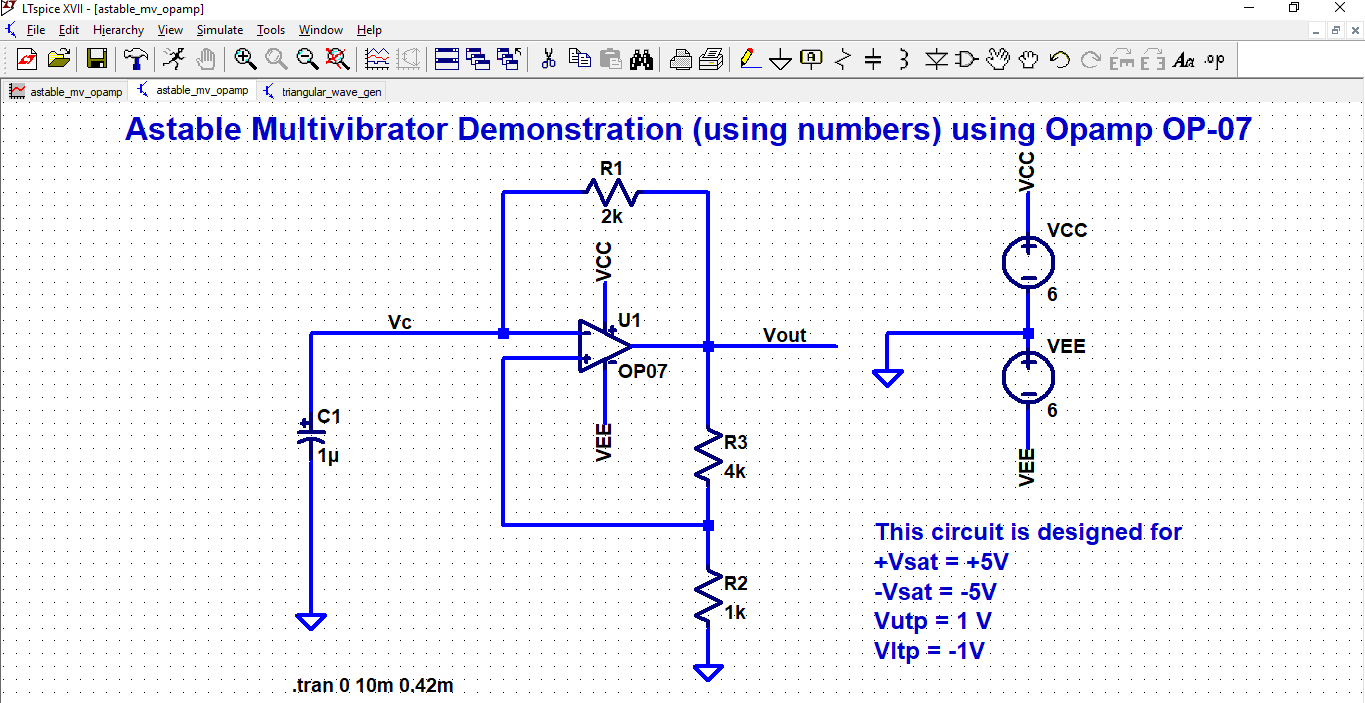
SIMULATION 25.02 : Output Waveform's for Astable multivibrator/square wave generator using Opamp OP-07
Lecture 26 handout dated 12-09-2018
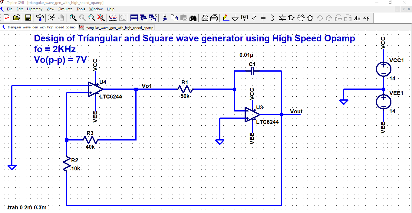
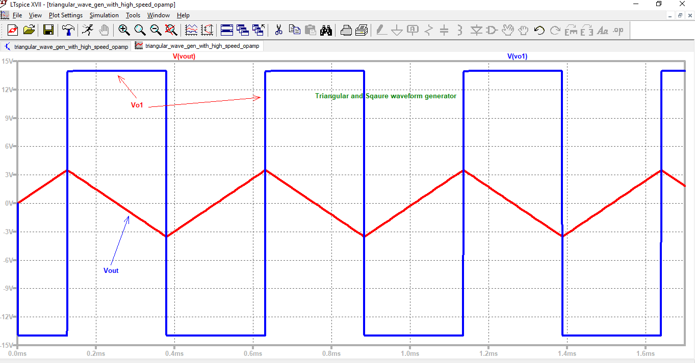
Topics Covered: Approach of Reverse Engineering adopted, Design of Triangular waveform generator circuit (with LT Spice simulation verification), then exploring the waveform of the circuit, then by analysis of the circuit with design values, working of the triangular wave generator was discussed along with the derivation of frequency of waveform.
Topics Covered: Approach of Reverse Engineering adopted, Design of Triangular waveform generator circuit (with LT Spice simulation verification), then exploring the waveform of the circuit, then by analysis of the circuit with design values, working of the triangular wave generator was discussed along with the derivation of frequency of waveform.
| licd_26.pdf |
SIMULATIONS related to lecture 26 are below : 26.01 to 26.04 ( Total 04 images)
SIMULATIONS related to lecture 26 are below : 26.01 to 26.04 ( Total 04 images)
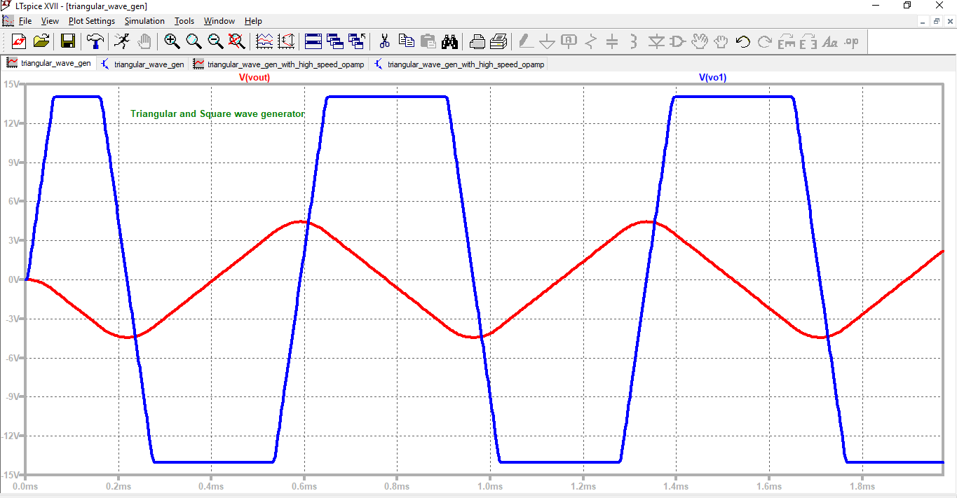
SIMULATION 26.01 : Design Circuit of Triangular and square wave generator using High Speed OPAMP
SIMULATION 26.02 : Waveform's of Triangular and square wave generator using HIGH Speed opamp
One can observe very sharp output triangular waveform's, and a perfect square wave ( That's what you get when you use high speed Opamp( i.e opamp with high Slew rate) )
One can observe very sharp output triangular waveform's, and a perfect square wave ( That's what you get when you use high speed Opamp( i.e opamp with high Slew rate) )
SIMULATION 26.03 : Design Circuit of Triangular and square wave generator using Low Speed OPAMP OP-07
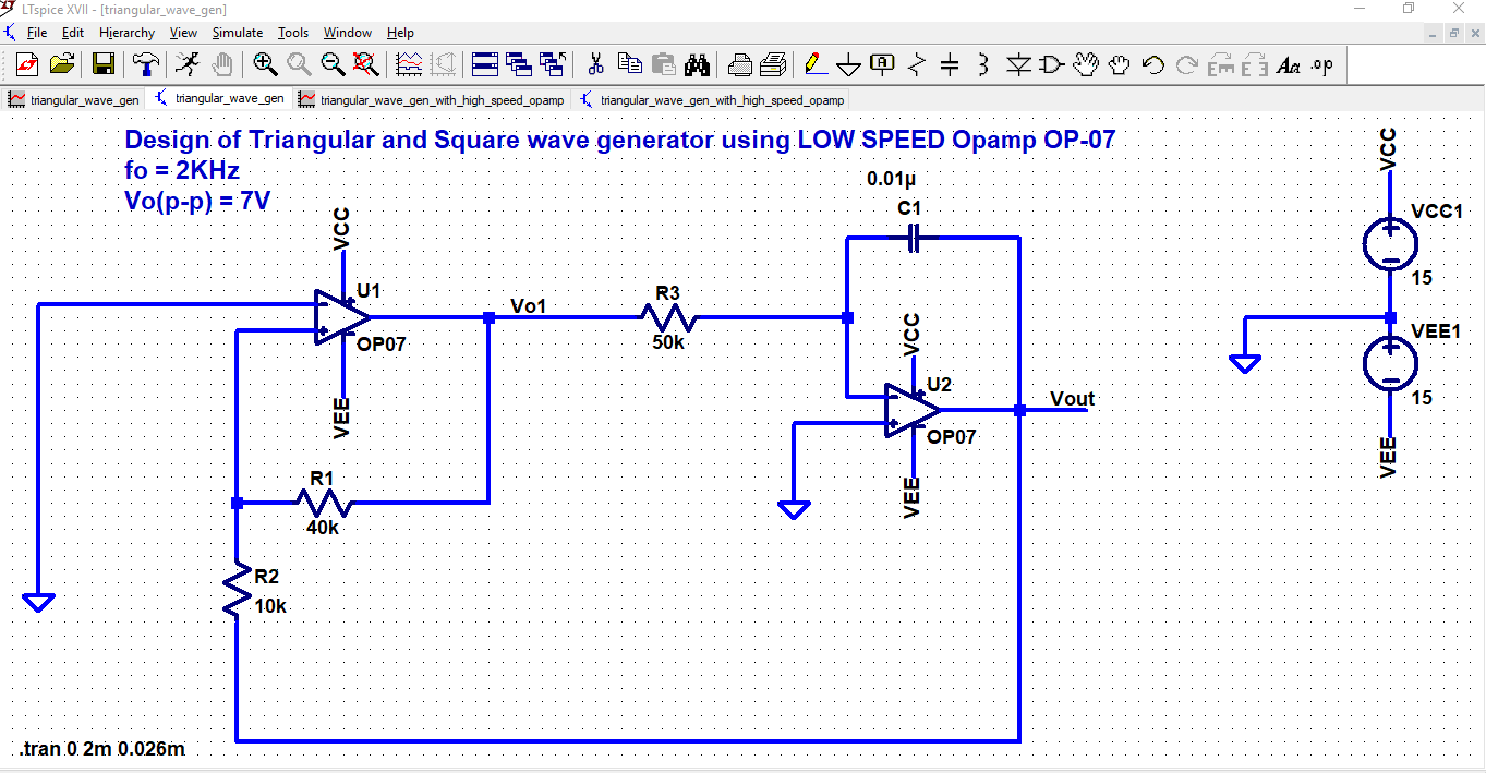
SIMULATION 26.04 : Waveform's of Triangular and square wave generator using LOW Speed opamp
One can observe not so sharp output triangular waveform's , and a square wave with finite slope ( That's what you get when you use Low speed Opamp( i.e opamp with low Slew rate) )
One can observe not so sharp output triangular waveform's , and a square wave with finite slope ( That's what you get when you use Low speed Opamp( i.e opamp with low Slew rate) )
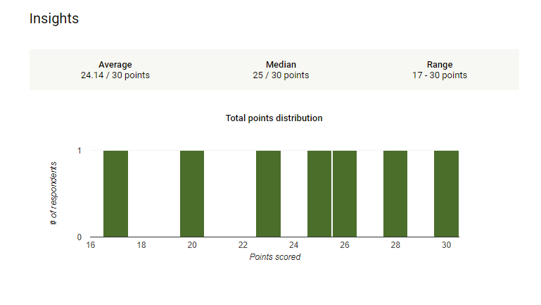
LICD MID TERM TEST 1 Marks and Analysis:
a) Total : 69 student appeared for the Midterm 1 test
b) 2 students scored perfect 30 marks
c) 5 (7%) out of 69 students scored more than 27 (90%) marks
d) 29 (42%) out of 69 students scored more than 15 (50%) marks
e) 8 ( 12%) out of 69 students scored between 12 to 14 marks
f) 22 (32%) out of 69 students scored less than 12 (40 %) marks
| ty_semv_test_1_result_september_2018.pdf |
End of Week 09: 11-09-2018 to 12-09-2018
Total no. of Lectures conducted: 02
Total Hours: 02
Activities during week 09:
1) Concepts: Demonstrated in LT Spice schematic and simulation tool
2) Numerical examples: Demonstrated in LT Spice schematic and simulation tool
4) Reverse engineering approach (for circuits) was adopted in Live class, i.e first design was discussed, then working with numerical values and then waveform's were drawn and verified in LT Spice
5) Concept working was explained with the help of numerical examples.
6) Video was shown as motivation for introducing a topic e.g Astable multi-vibrator
Announcement as on 16-9-2018
LICD test 1 papers will shown to students during working hours between 9:30 to 5 pm from 17-9-2018 to 21-9-2018 excluding holidays
Announcement as on 16-9-2018
LICD test 1 papers will shown to students during working hours between 9:30 to 5 pm from 17-9-2018 to 21-9-2018 excluding holidays
Lecture 27 handout dated 18-09-2018
Topics Covered: Design of Square wave generator using opamp (with LT Spice simulation and verification of the design), concept of Voltage limiting in square wave generator and triangular waveform generator circuit (with LT Spice simulation of the circuit), Use of clock in digital system, Revisited 3 opamp Instrumentation amplifier and its formula + LT Spice simulation, Disadvantages of 3 opamp IA of using 7 external resistors, Necessity of Instrumentation amplifier Monolithic IC AD620 ( Single gain Programmable Instrumentation amplifier + with LT Spice simulation of the circuit)
Topics not covered: AD620 brief discussion
| licd_27.pdf |
SIMULATIONS related to lecture 27 are below : 27.01 to 27.09 ( Total 09 images)
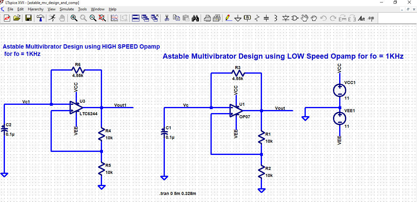
SIMULATION 27.01 : Design Circuit of square wave generator and comparison of using High Speed OPAMP with LOW speed opamp
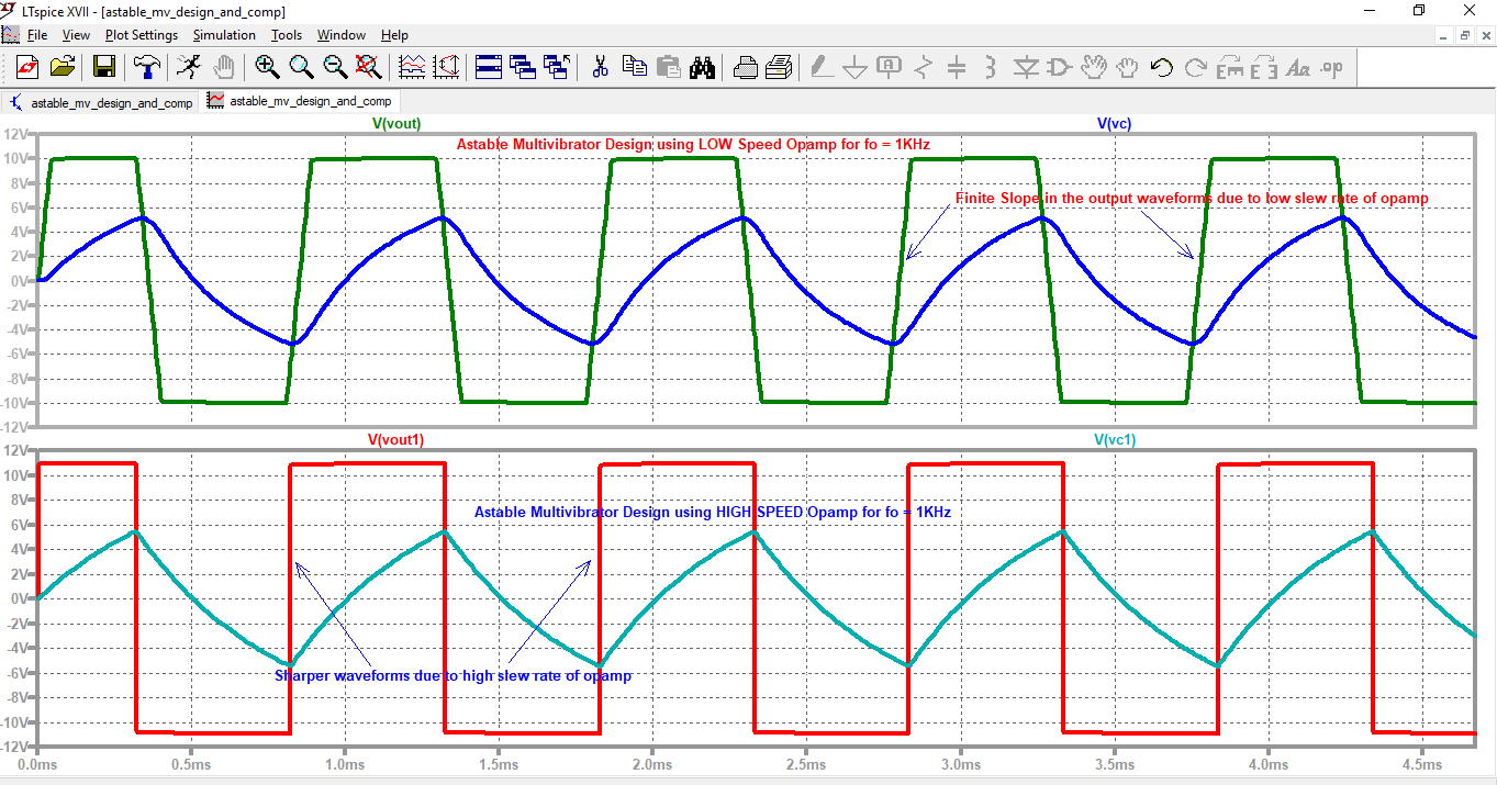
SIMULATION 27.02 : Waveform's for square wave generator and comparison of using High Speed OPAMP with LOW speed opamp
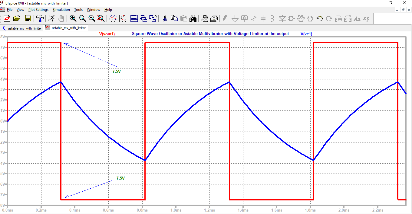
SIMULATION 27.03 : Design Circuit of square wave generator/ oscillator with Voltage limiter at the output
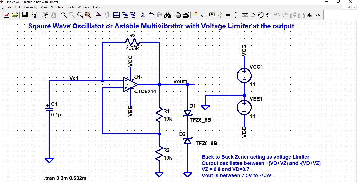
SIMULATION 27.04 : Waveform's for square wave generator with voltage limiter at its output
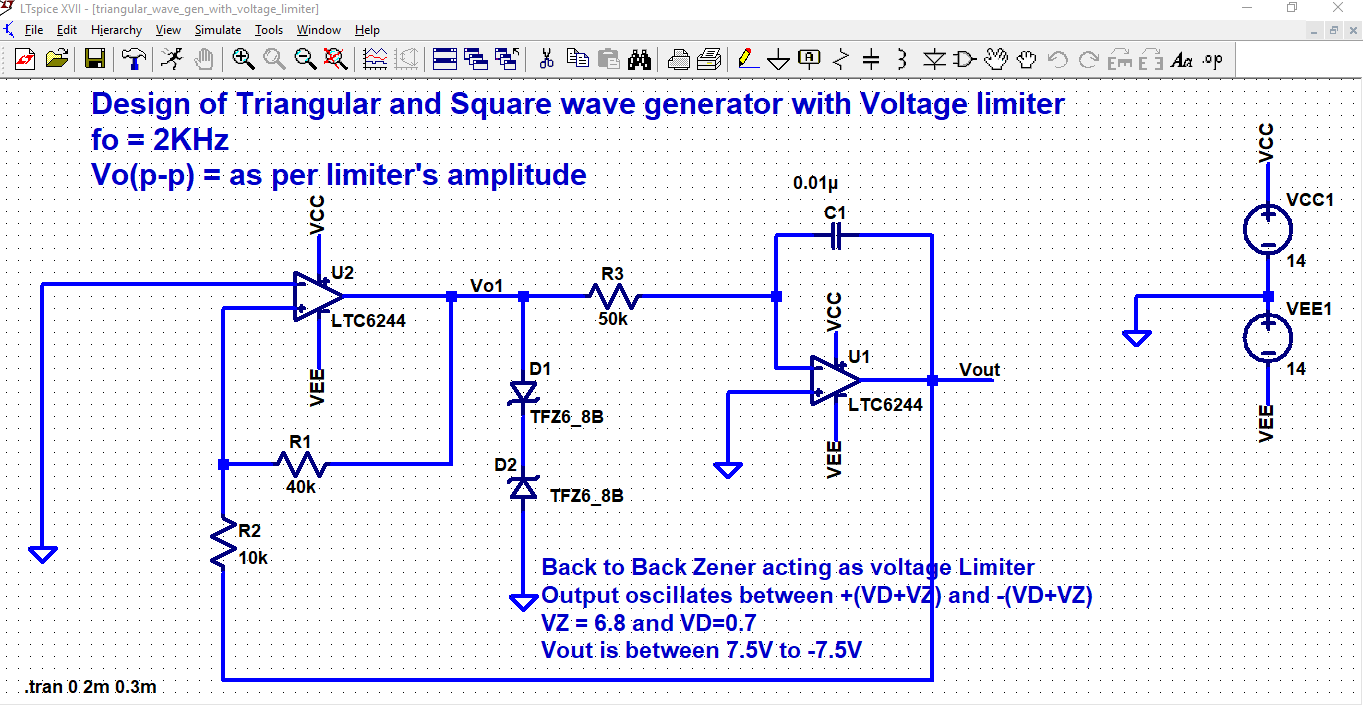
SIMULATION 27.05 : Design Circuit for Triangular and square wave generator with output Limiter
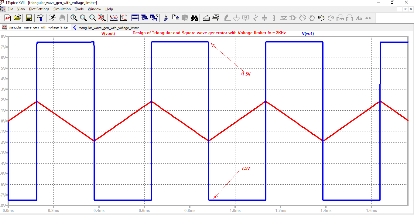
SIMULATION 27.06 : Waveform's of Triangular and square wave generator with output Limiter
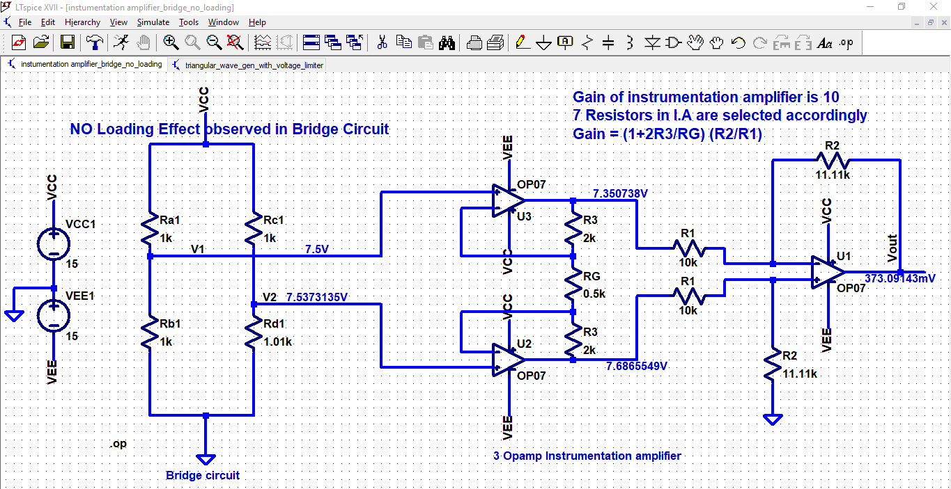
SIMULATION 27.07 : Revisited 3 opamp Instrumentation amplifier and commented that to set a fixed precise gain, we need 7 external resistors of closely matched and accurate values (which is never practically realizable.... That's why we go for Instrumentation amplifier IC
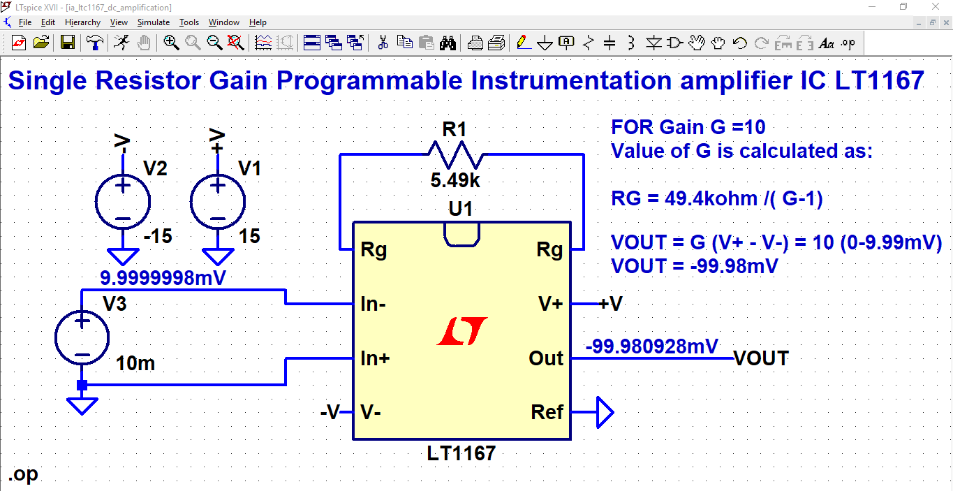
SIMULATION 27.08 : Single resistor programmable Instrumentation amplifier LT 1167 demonstration in amplifying 10 mV DC signal with a Gain of 10 with single external resistor RG
NOTE: In syllabus, Instrumentation amplifier IC AD 620 is mentioned, but here we are using LTC1167 as it is available in LT Spice library, because both the ICs have almost similar features (almost no difference between the two) and moreover, in LT SPICE library AD620 is not present.
NOTE: In syllabus, Instrumentation amplifier IC AD 620 is mentioned, but here we are using LTC1167 as it is available in LT Spice library, because both the ICs have almost similar features (almost no difference between the two) and moreover, in LT SPICE library AD620 is not present.
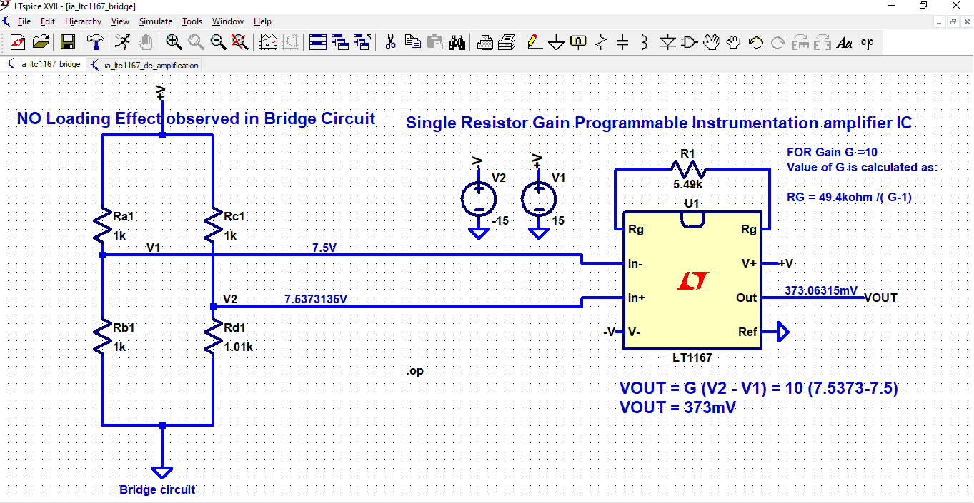
SIMULATION 27.08 : Single resistor programmable Instrumentation amplifier LT 1167 demonstration with Bridge circuit amplifying with a Gain of 10 with single external resistor RG and we achieve accurate results as compared as compared to simulation 27.06 and that too just by using single external resistor RG
NOTE: In syllabus, Instrumentation amplifier IC AD 620 is mentioned, but here we are using LTC1167 ( only for simulation purposes)
NOTE: In syllabus, Instrumentation amplifier IC AD 620 is mentioned, but here we are using LTC1167 ( only for simulation purposes)
Video related to lecture 27 is below : 27.01 (Total 1)
Video 27.01 : MIT lecture on Why use a Clock in Digital Systems ?
Lecture 28 handout dated 19-09-2018: uploaded on 23-9-2018 by 11:55 pm
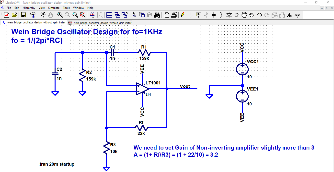
Topics Covered: Approach of Reverse Engineering adopted, Design of Wien bridge oscillator circuit (with LT Spice simulation verification), then exploring the waveform of the circuit, working conditions of Wien bridge oscillator circuit discussed and derivation of it's frequency of oscillations and amplitude were derived in class.
Topics Covered: Approach of Reverse Engineering adopted, Design of Wien bridge oscillator circuit (with LT Spice simulation verification), then exploring the waveform of the circuit, working conditions of Wien bridge oscillator circuit discussed and derivation of it's frequency of oscillations and amplitude were derived in class.
| licd_28.pdf |
SIMULATIONS related to lecture 28 are below : 28.01 to 28.05 ( Total 05 images)
SIMULATION 28.01 : Wein Bridge Oscillator Circuit Design
SIMULATION 28.02 : Output sinusoidal Waveform's for Designed Wein Bridge Oscillator
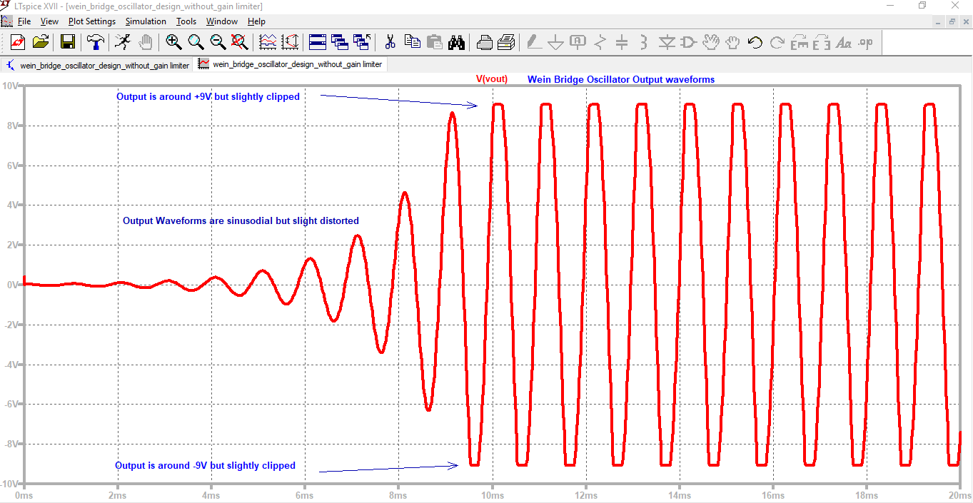
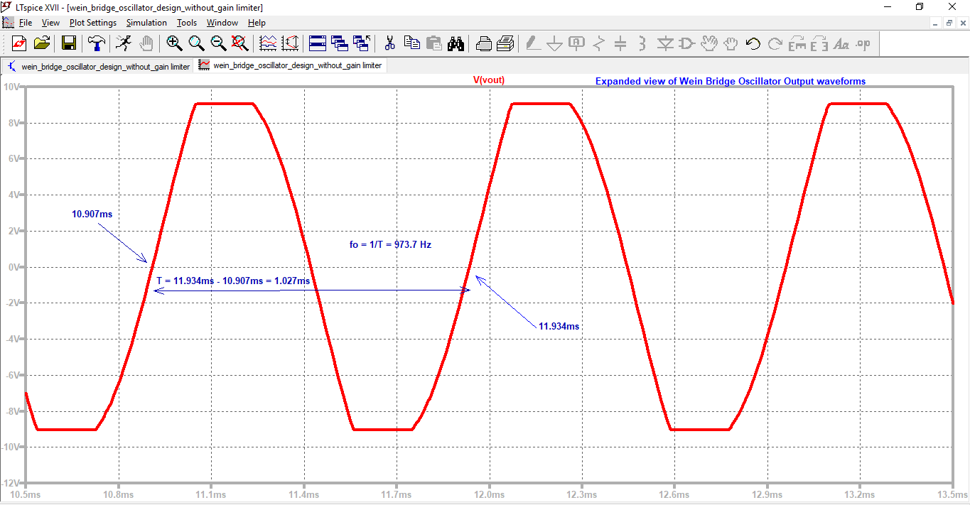
SIMULATION 28.03 : Expanded View of Output sinusoidal Waveform's for Designed Wein Bridge Oscillator
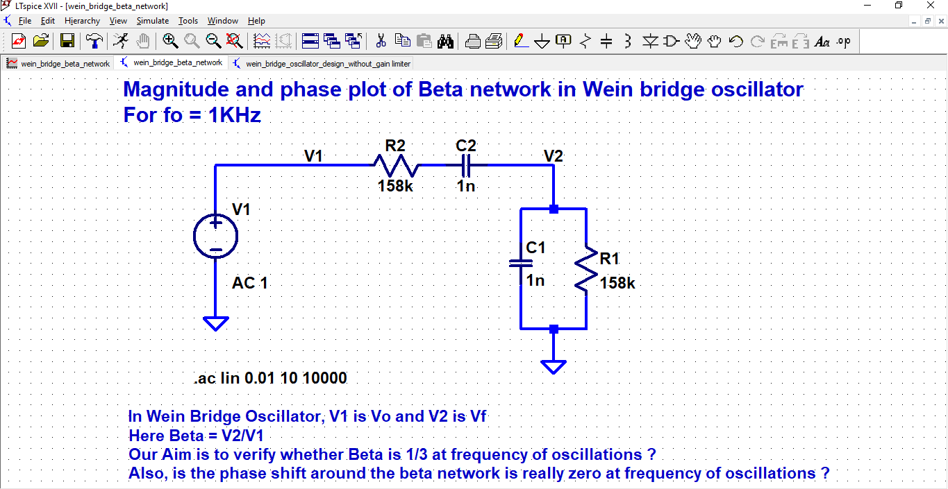
SIMULATION 28.04 : Beta Network Circuit in Wein Bridge Oscillator
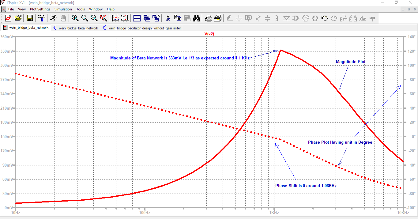
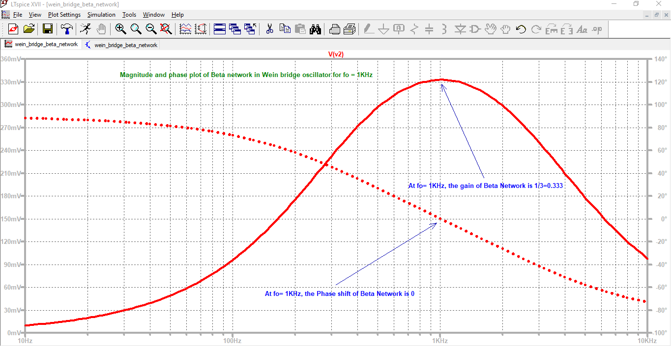
SIMULATION 28.05 : Magnitude and Phase Plot of Beta Network Circuit in Wein Bridge Oscillator
Video related to lecture 28 is below : 28.01 (Total 1)
Video 28.01 : IITB lecture on Wien Bridge Oscillator
start video from beginning and watch it till 13 minutes and 55 seconds
start video from beginning and watch it till 13 minutes and 55 seconds
Lecture 29 handout dated 21-09-2018: uploaded on 24-9-2018 by 1:15 am
Topics Covered: The SIMULATION 28.05 : Magnitude and Phase Plot of Beta Network Circuit in Wein Bridge Oscillator was refined and discussed in the class, Remedy to Problem of Amplitude stabilization in WBO circuit was also discussed in details and shown in LT spice simulation, Design of RC phase Shift Oscillator with hand- calculations and verification with the help of LT Spice simulation.
PS: Few Minutes were wasted during the lecture 29 will be compensated in subsequent lectures.
| licd_29.pdf |
SIMULATIONS related to lecture 29 are below : 29.01 to 29.05 ( Total 05 images)
SIMULATION 29.01 : Refinement over Simulation 28.06 waveform's i.e Magnitude and Phase Plot of Beta Network Circuit in Wein Bridge Oscillator
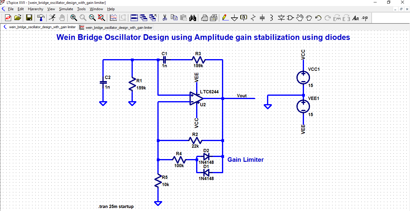
SIMULATION 29.02 : Wein Bridge Oscillator Designed Circuit with Amplitude gain Stabilization
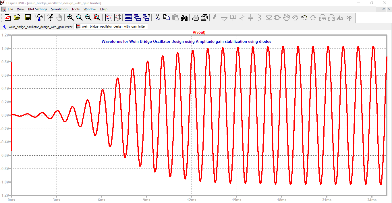
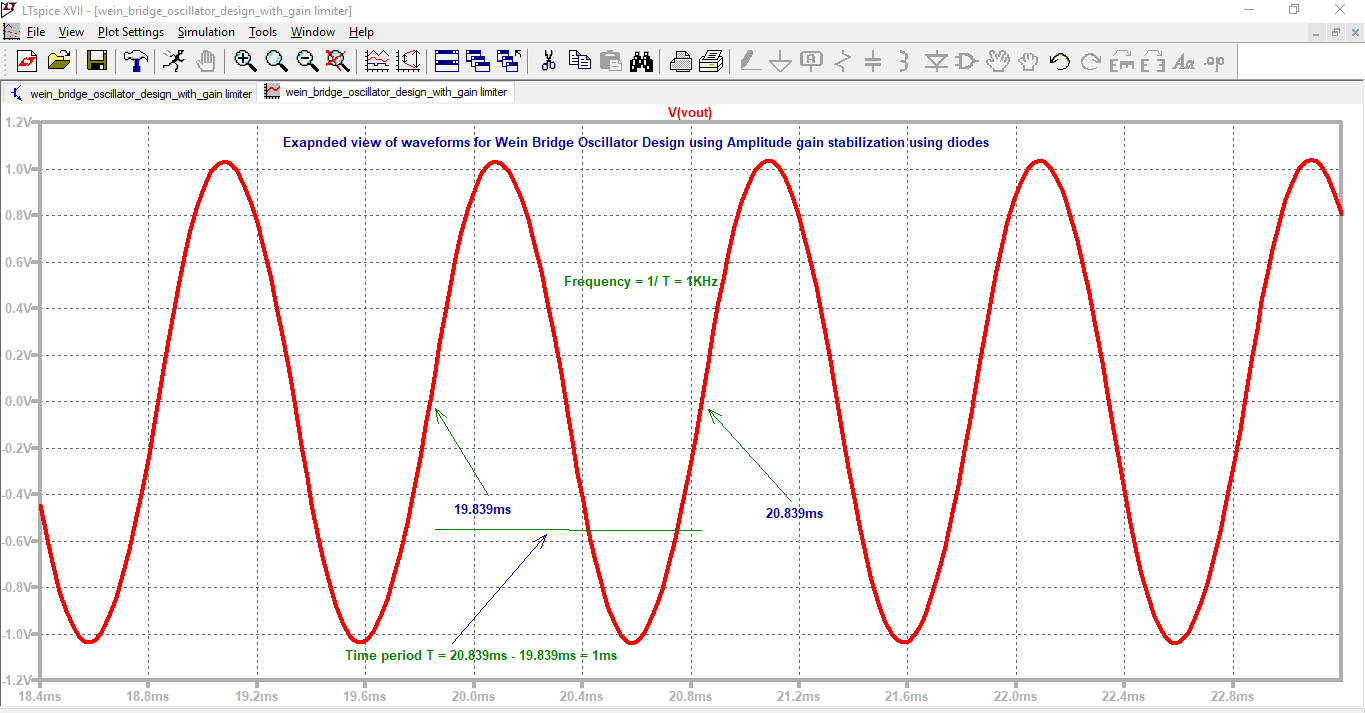
SIMULATION 29.03 : Output Waveform for Wein Bridge Oscillator with Amplitude gain Stabilization
SIMULATION 29.04 : Expanded view of Output Waveform for Wein Bridge Oscillator with Amplitude gain Stabilization
SIMULATION 29.05 : RC Phase Shift Oscillator designed Circuit for fo= 100Hz
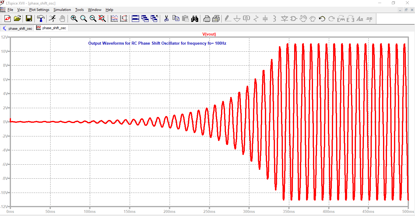
SIMULATION 29.06 : Output Waveform's for RC Phase Shift Oscillator for fo=100Hz
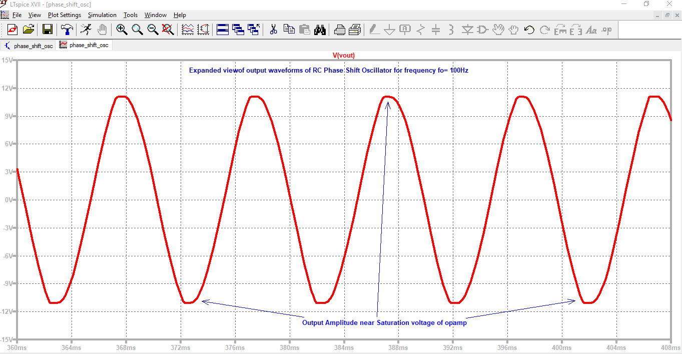
SIMULATION 29.07 : Expanded view of Output Waveform's for RC Phase Shift Oscillator for fo=100Hz
End of Week 10: 18-09-2018 to 21-09-2018
Total no. of Lectures conducted: 03
Total Hours: 03
Activities during week 10:
1) Concepts: Demonstrated in LT Spice schematic and simulation tool
2) Numerical examples: Demonstrated in LT Spice schematic and simulation tool
4) Reverse engineering approach (for circuits) was adopted in Live class, i.e first design was discussed, then working with numerical values and then waveform's were drawn and verified in LT Spice
5) Concept working was explained with the help of numerical examples.
Lecture 30 handout dated 26-09-2018: updated on 28/9/2018 at 10:40 pm
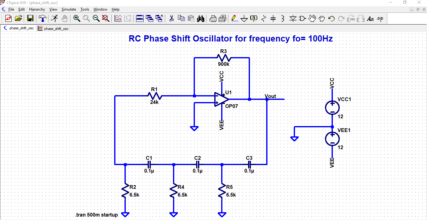
Topics Covered: Working of RC phase shift oscillator, Analysis (i.e derivation steps for fo and gain of beta network) of Beta network of RC phase Shift Oscillator with verification in LT Spice simulation, discussion on Need for Amplitude control of Output oscillations in Phase oscillator circuit, Non-linear amplitude control in Phase shift oscillator with verification in LT Spice simulation.
Topics Covered: Working of RC phase shift oscillator, Analysis (i.e derivation steps for fo and gain of beta network) of Beta network of RC phase Shift Oscillator with verification in LT Spice simulation, discussion on Need for Amplitude control of Output oscillations in Phase oscillator circuit, Non-linear amplitude control in Phase shift oscillator with verification in LT Spice simulation.
| licd_30.pdf |
SIMULATIONS related to lecture 30 are below : 30.01 to 30.08 ( Total 08 images)
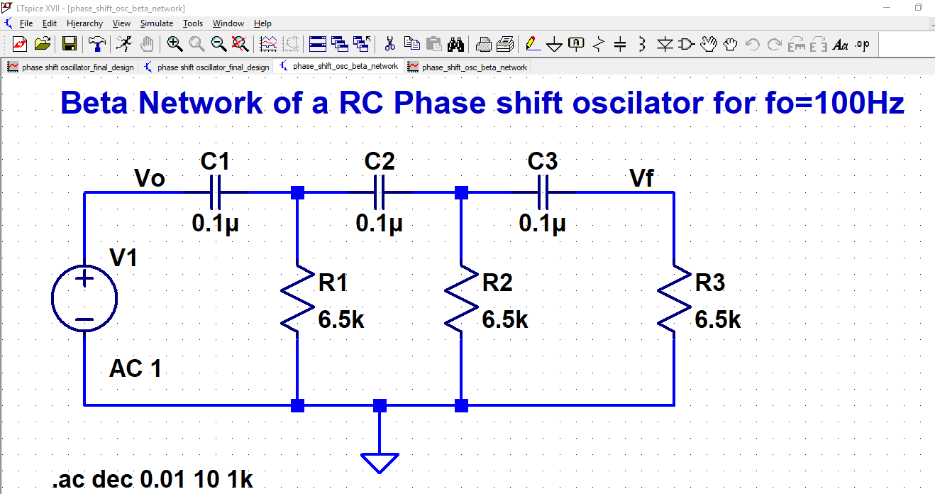
SIMULATION 30.01 : Beta network of a RC Phase Shift Oscillator for fo= 100Hz
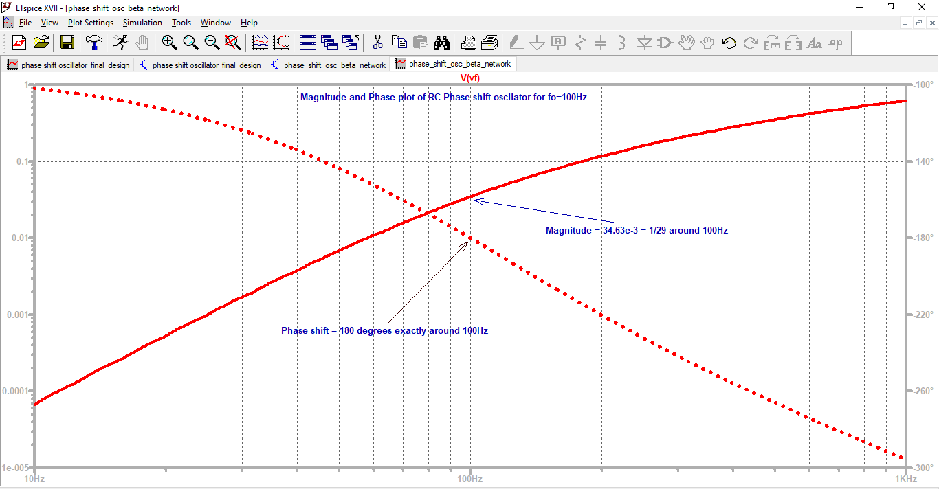
SIMULATION 30.02 : Magnitude and Phase plot of Beta network for a RC Phase Shift Oscillator for fo= 100Hz
One can clearly observe that, exactly at fo=100Hz, the phase shift of beta network is 180 degrees and its gain is around 1/29
One can clearly observe that, exactly at fo=100Hz, the phase shift of beta network is 180 degrees and its gain is around 1/29
SIMULATION 30.03 : Limiter circuit with Output gain control
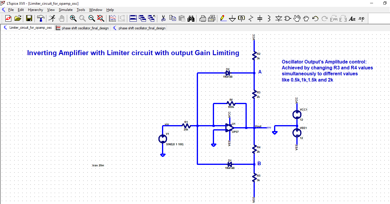
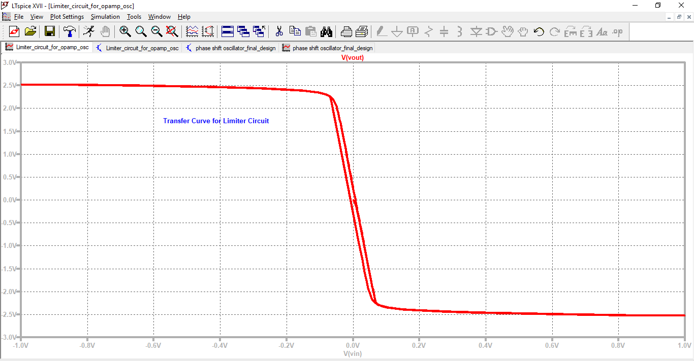
SIMULATION 30.04 : Transfer curve for a Limiter circuit with Output gain control
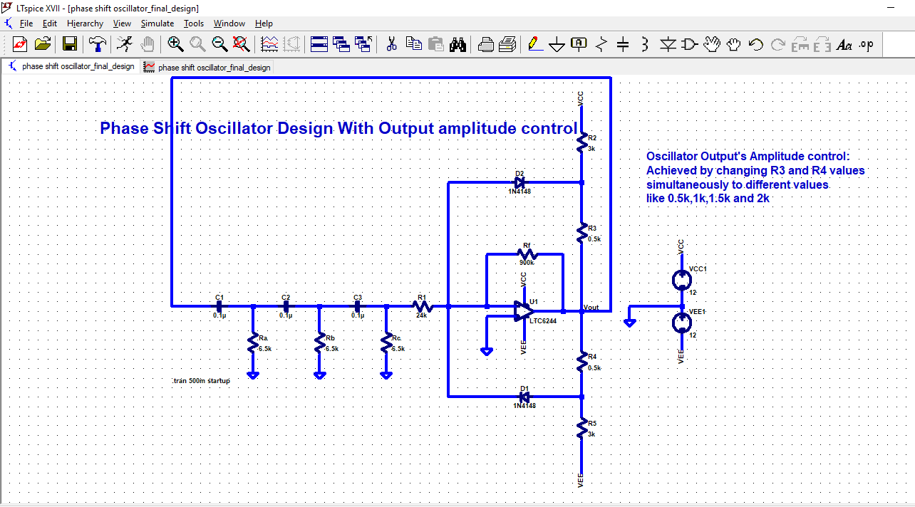
SIMULATION 30.05 : Phase shift oscillator design with Output amplitude control
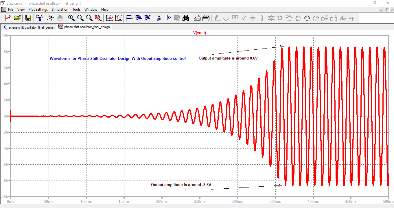
SIMULATION 30.06 : Waveform's of Phase shift oscillator design with Output amplitude control between 8.6 V and -8.6 V
SIMULATION 30.07 : Waveform's of Phase shift oscillator design with Output amplitude control between 2.33 V and -2.33 V
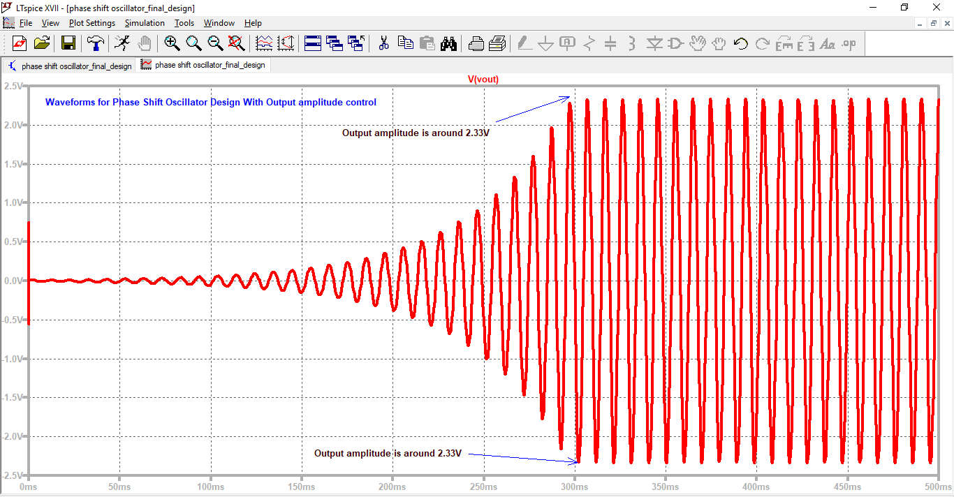
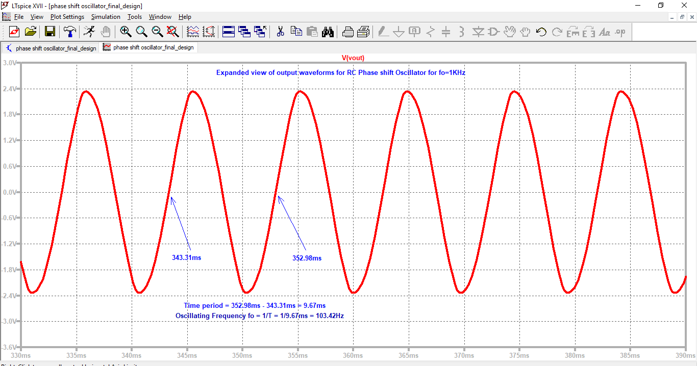
SIMULATION 30.08 : Expanded view of Waveform of Phase shift oscillator design with Output amplitude control between 2.33 V and -2.33 V with observed frequency of oscillation as 103.42Hz
Lecture 31 handout dated 27-09-2018: uploaded on 29/08/2018 by 11:32 pm
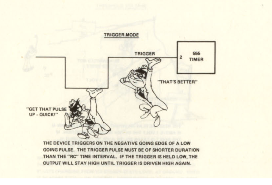
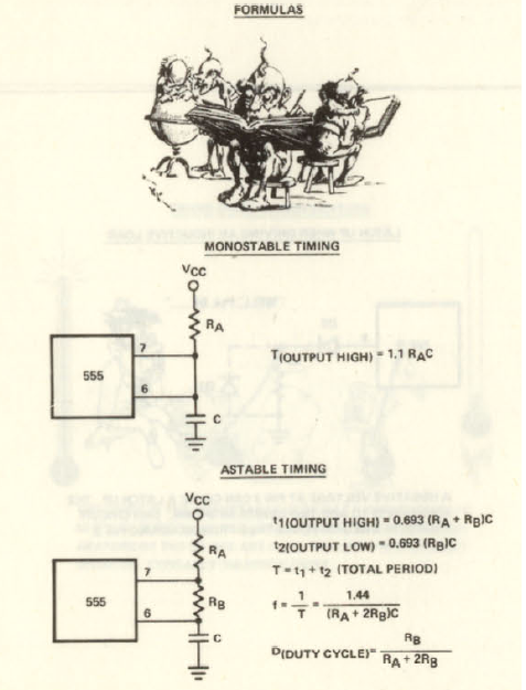
Topics Covered: Introduction to Timer IC 555, Functional block diagram of 555 timer, 555 as mono-stable multivibrator working with functional block diagram and waveforms, derivation of output pulse width T, Design of Mono-stable multivibrator using 555 timer and it's verification in LT Spice simulation.
Topics Covered: Introduction to Timer IC 555, Functional block diagram of 555 timer, 555 as mono-stable multivibrator working with functional block diagram and waveforms, derivation of output pulse width T, Design of Mono-stable multivibrator using 555 timer and it's verification in LT Spice simulation.
| licd_31.pdf |
Video related to lecture 31 is below : 31.01 (Total 1)
Video 31.01 : IITB lecture on 555 timer, Functional block and monostable multivibrator working using functional block diagram
Start video from beginning and watch it till 14 minutes and 25 seconds
Start video from beginning and watch it till 14 minutes and 25 seconds
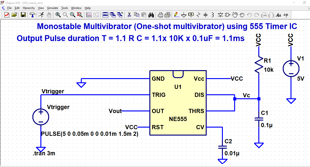
SIMULATIONS related to lecture 31 are below : 31.01 to 31.02 ( Total 02 images)
SIMULATION 31.01 : Mono-stable multivibrator circuit using 555 timer IC designed for output pulse duration of T=1.1 ms
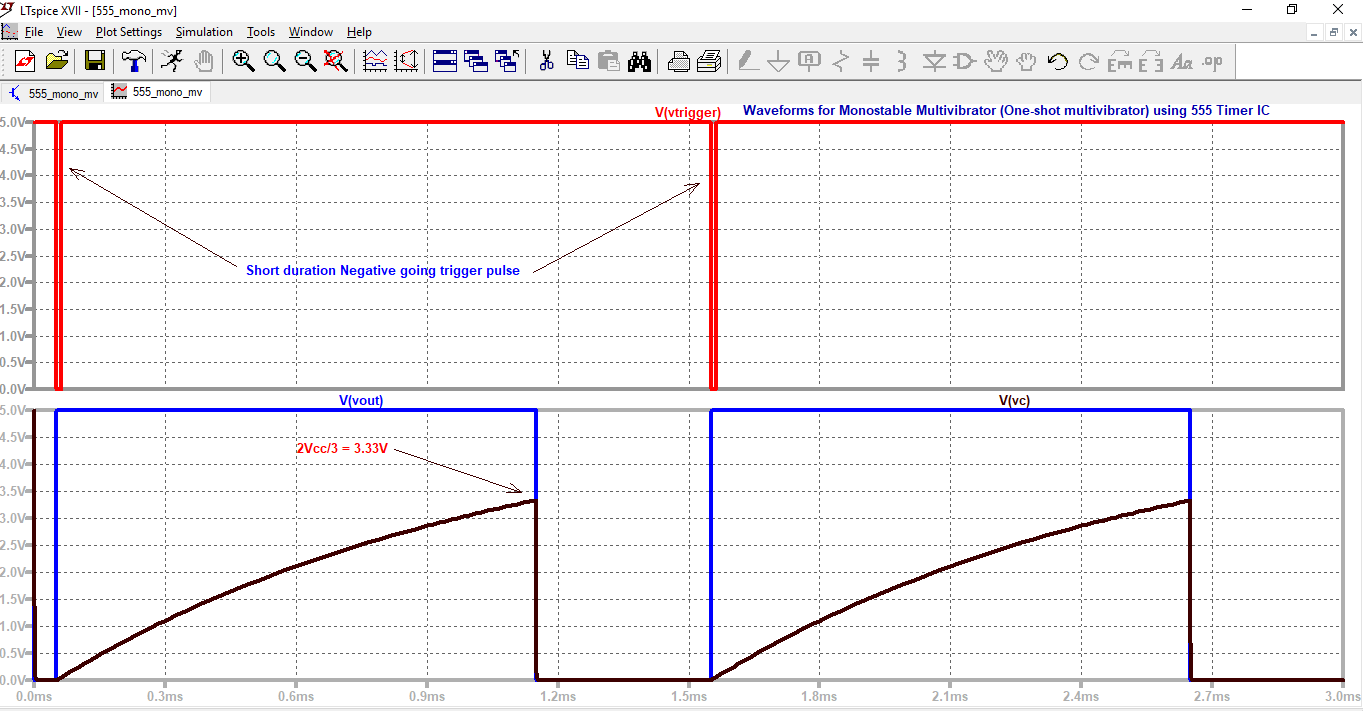
SIMULATION 31.02 : Waveform's for Mono-stable multivibrator using 555 timer IC designed for output pulse duration of T=1.1 ms
ANIMATION LINKS related to lecture 31 are below :
ANIMATION LINK 01 : Screen Shot view of the link
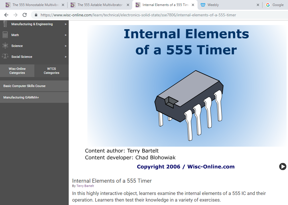
https://www.wisc-online.com/learn/technical/electronics-solid-state/sse7806/internal-elements-of-a-555-timer
ANIMATION LINK 02 : Screen Shot view of the link
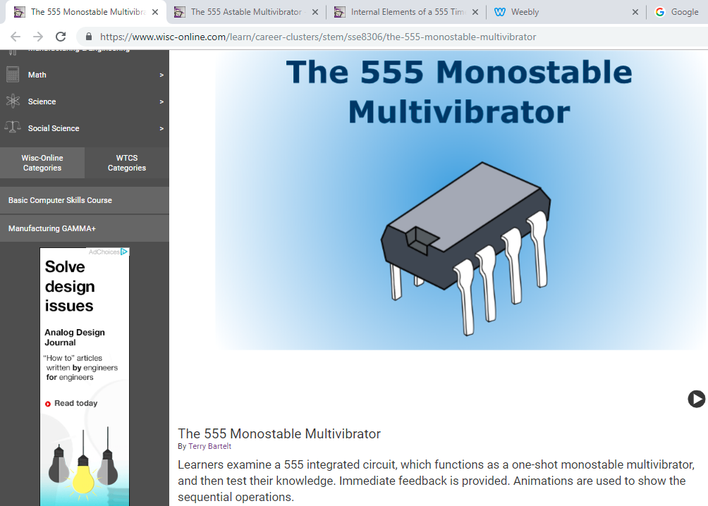
https://www.wisc-online.com/learn/career-clusters/stem/sse8306/the-555-monostable-multivibrator
https://www.wisc-online.com/learn/career-clusters/stem/sse8306/the-555-monostable-multivibrator
Lecture 32 handout dated 28-09-2018: uploaded on 29/9/2018 by 11:52 pm
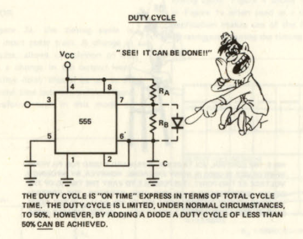
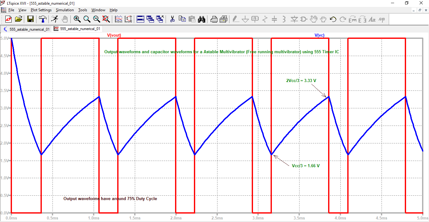
Topics Covered: 555 as Astable multivibrator working with functional block diagram and waveforms, derivation of t high and t low, % duty cycle for astable multivibrator, Numerical discussed in class on Astable multivibrator using 555 timer and it's verification in LT Spice simulation and hands-on calculations.
Topics Covered: 555 as Astable multivibrator working with functional block diagram and waveforms, derivation of t high and t low, % duty cycle for astable multivibrator, Numerical discussed in class on Astable multivibrator using 555 timer and it's verification in LT Spice simulation and hands-on calculations.
| licd_32.pdf |
Video related to lecture 32 is below : 32.01 (Total 1)
Video 32.01 : IITB lecture on 555 timer, Functional block and monostable multivibrator working using functional block diagram
Start video from 17 minutes and 22 seconds and watch it till 22 minutes and 10 seconds
Start video from 17 minutes and 22 seconds and watch it till 22 minutes and 10 seconds
SIMULATIONS related to lecture 32 are below : 32.01 to 32.02 ( Total 02 images)
SIMULATION 32.01 : Astable multivibrator circuit using 555 timer IC
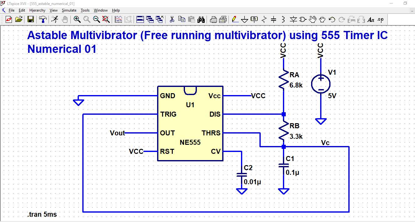
SIMULATION 32.02 : Waveform's of Astable multivibrator circuit using 555 timer IC
ANIMATION LINKS related to lecture 32 are below :
ANIMATION LINK 01 : Screen Shot view of the link
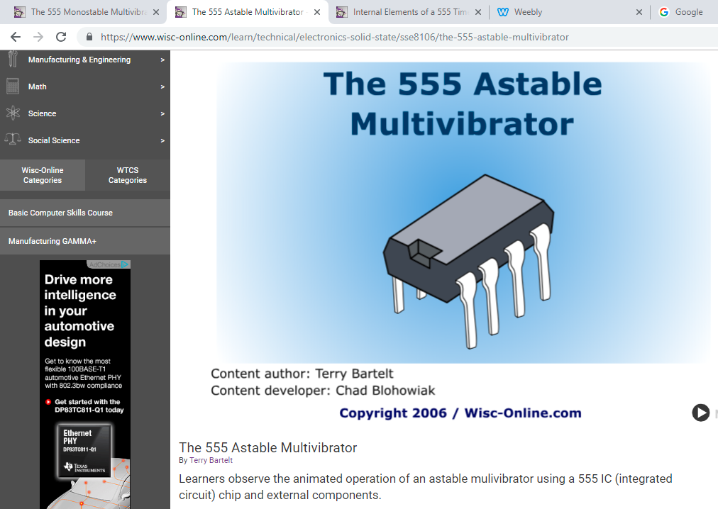
https://www.wisc-online.com/learn/technical/electronics-solid-state/sse8106/the-555-astable-multivibrator
https://www.wisc-online.com/learn/technical/electronics-solid-state/sse8106/the-555-astable-multivibrator
End of Week 11: 26-09-2018 to 28-09-2018
Total no. of Lectures conducted: 03
Total Hours: 03
Activities during week 11:
1) Concepts: Demonstrated in LT Spice schematic and simulation tool
2) Numerical examples: Demonstrated in LT Spice schematic and simulation tool
3) Some topics were covered in traditional approach while some topics were covered using Animations.
4) Concept working was explained with the help of numerical examples.
Lecture 33 handout dated 03-10-2018: uploaded on 7/10/2018 by 11:52 pm
Topics Covered: Design of Astable multivibrator using 555 timer for 75% Duty Cycle, 50% duty cycle and less than 50% duty cycle and it's verification in LT Spice simulation with hands-on calculations. Revisited Mono-stable multivibrator circuit and discussed three applications based on mono-stable multivibrator using 555; a) Frequency divider b) Linear Ramp generator c) Pulse width modulation and its simulations waveforms in LT Spice were discussed with students
Topics Covered: Design of Astable multivibrator using 555 timer for 75% Duty Cycle, 50% duty cycle and less than 50% duty cycle and it's verification in LT Spice simulation with hands-on calculations. Revisited Mono-stable multivibrator circuit and discussed three applications based on mono-stable multivibrator using 555; a) Frequency divider b) Linear Ramp generator c) Pulse width modulation and its simulations waveforms in LT Spice were discussed with students
| licd_33.pdf |
SIMULATIONS related to lecture 33 are below : 33.01 to 33.12 ( Total 12 images)
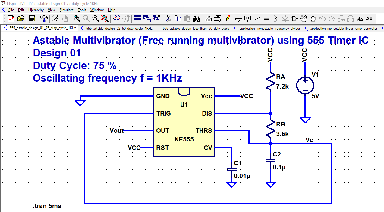
SIMULATION 33.01 : Designed Astable multivibrator circuit using 555 timer IC for 75% duty cycle and 1 kHz frequency
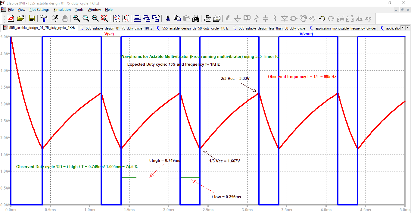
SIMULATION 33.02 : Waveform for Designed Astable multivibrator circuit using 555 timer IC for 75% duty cycle and 1 kHz frequency
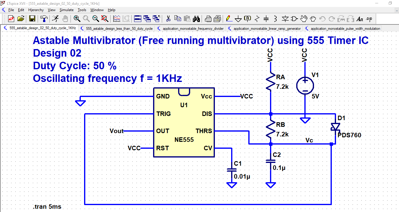
SIMULATION 33.03 : Designed Astable multivibrator circuit using 555 timer IC for 50% duty cycle and 1 kHz frequency
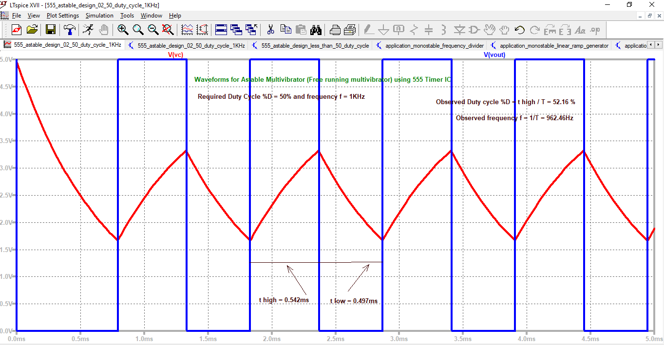
SIMULATION 33.04 : Waveform for Designed Astable multivibrator circuit using 555 timer IC for 50% duty cycle and 1 kHz frequency
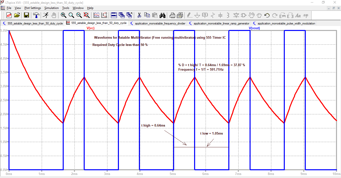
SIMULATION 33.05 : Designed Astable multivibrator circuit using 555 timer IC for less than 50% duty cycle
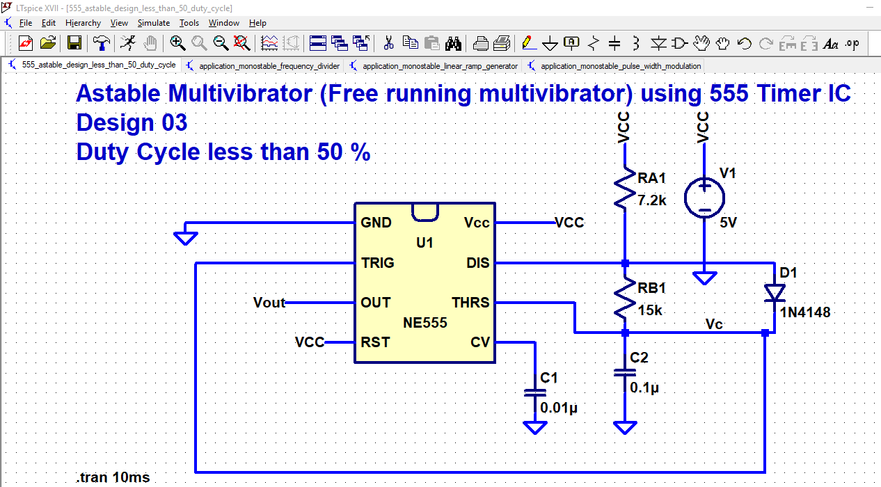
SIMULATION 33.06 : Designed Astable multivibrator circuit using 555 timer IC for less than 50% duty cycle
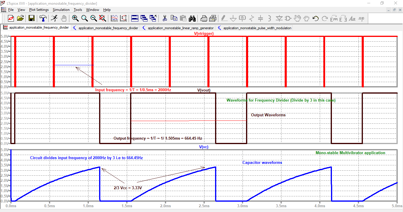
SIMULATION 33.07: Application of Mono-stable Multi-vibrator: Frequency Divider circuit
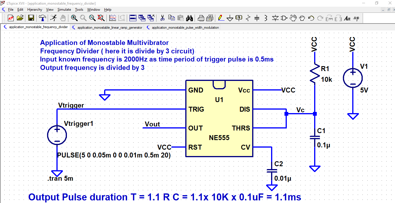
SIMULATION 33.08: Output waveforms for Frequency Divider circuit
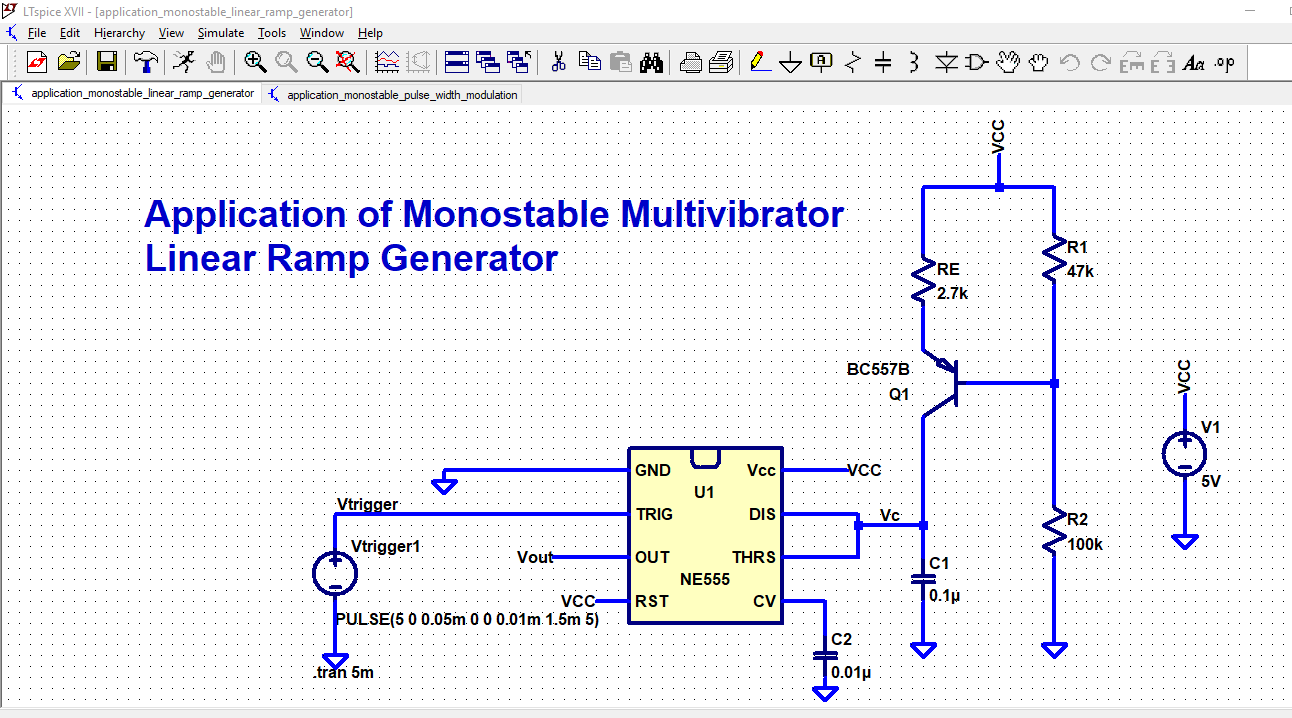
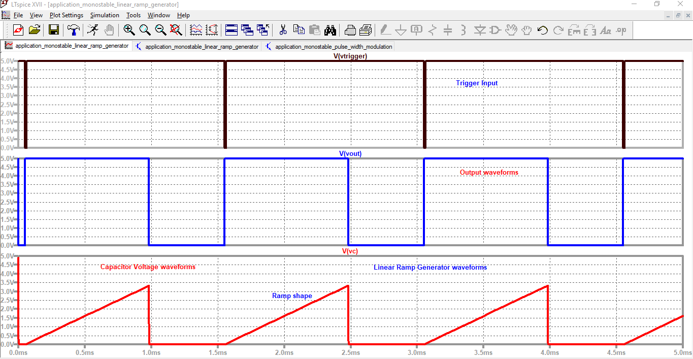
SIMULATION 33.09: Application of Mono-stable Multi-vibrator: Linear ramp generator circuit
SIMULATION 33.10: Waveform's for Linear ramp generator circuit
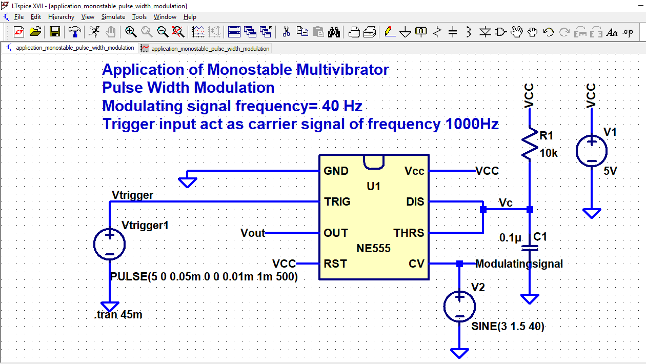
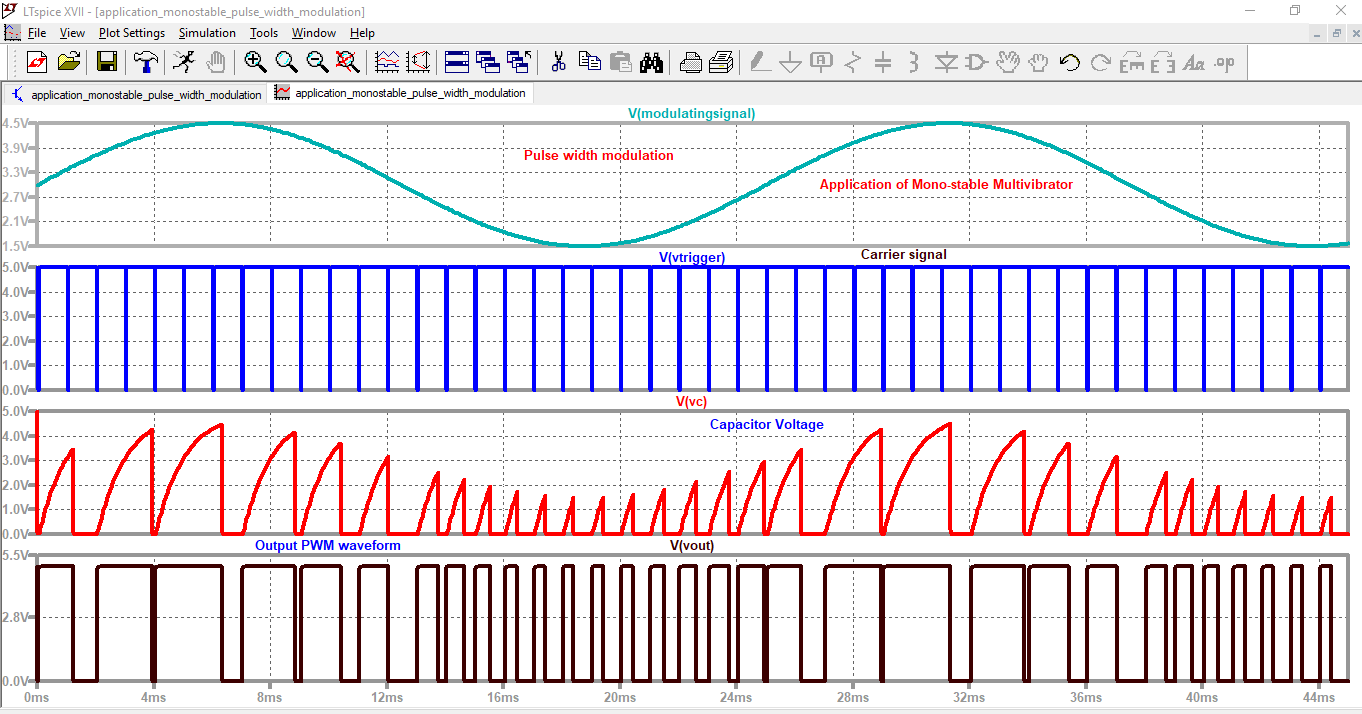
SIMULATION 33.11: Application of Mono-stable Multi-vibrator: Pulse width modulation circuit
SIMULATION 33.12: Waveform's for Pulse width modulation circuit
Lecture 34 handout dated 04-10-2018: uploaded on 24-10-2018 by 11:52 am
Topics Covered: Discussed three applications based on Astable multivibrator using 555; a) Schmitt trigger (Sine wave to square wave converter) b) Voltage Controlled oscillator (Voltage to frequency converter) c) Pulse Position modulation and its simulations waveforms in LT Spice were discussed with students
Topics Covered: Discussed three applications based on Astable multivibrator using 555; a) Schmitt trigger (Sine wave to square wave converter) b) Voltage Controlled oscillator (Voltage to frequency converter) c) Pulse Position modulation and its simulations waveforms in LT Spice were discussed with students
| licd_34.pdf |
SIMULATIONS related to lecture 34 are below : 34.01 to 34.11 ( Total 11 images)
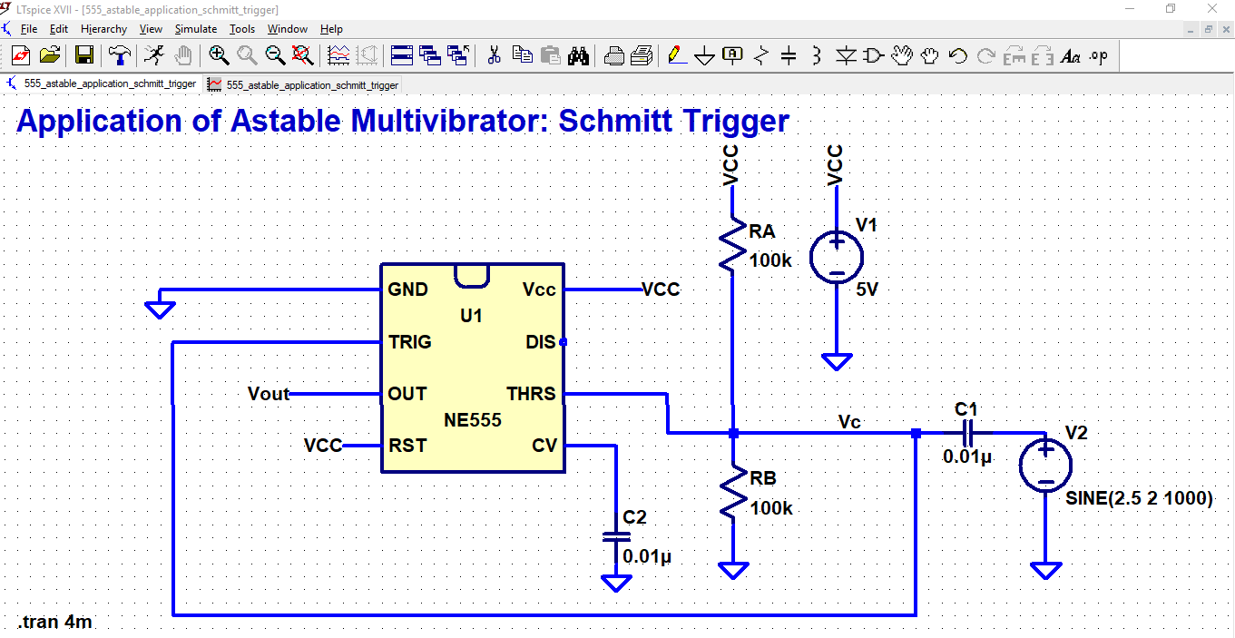
SIMULATION 34.01: Application of Astable Multi-vibrator: Schmitt trigger circuit
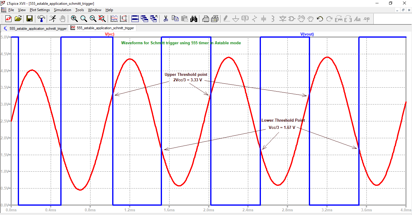
SIMULATION 34.02: Application of Astable Multi-vibrator: Waveform's for Schmitt trigger
One can observe square wave output w.r.t Upper threshold point and lower threshold point of input sine wave
One can observe square wave output w.r.t Upper threshold point and lower threshold point of input sine wave
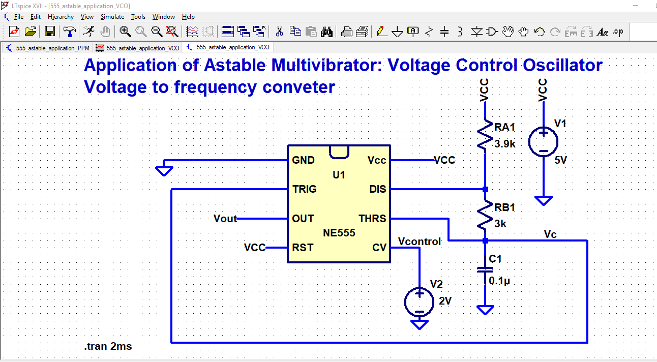
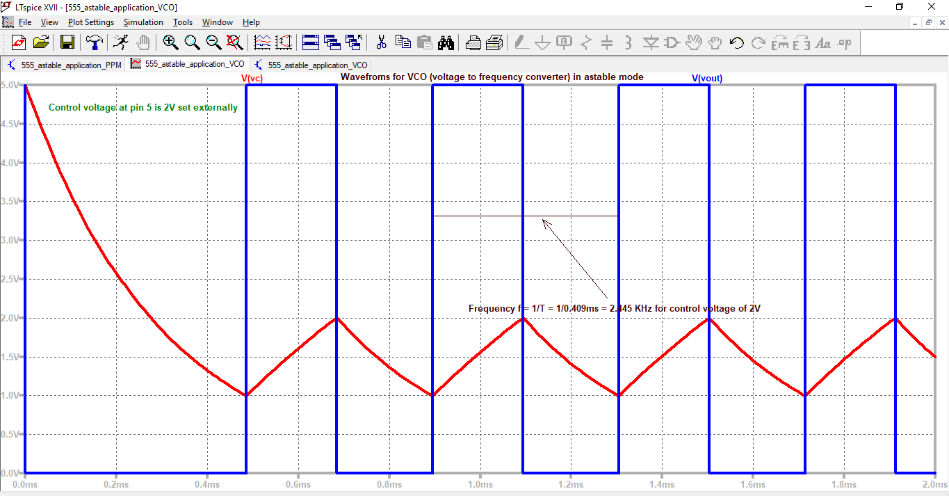
SIMULATION 34.03: Application of Astable Multi-vibrator: Voltage control oscillator (voltage to frequency) circuit
SIMULATION 34.04: Application of Astable Multi-vibrator: Waveform's for voltage control oscillator
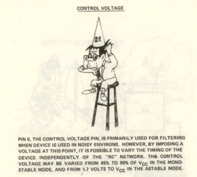
For control voltage of 2 V set externally, the output frequency is 2.445 KHz
For control voltage of 2 V set externally, the output frequency is 2.445 KHz
SIMULATION 34.05: Application of Astable Multi-vibrator: Waveform's for voltage control oscillator
For control voltage of 3 V set externally, the output frequency is 1.67 KHz
For control voltage of 3 V set externally, the output frequency is 1.67 KHz
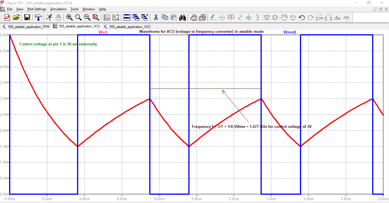
SIMULATION 34.06: Application of Astable Multi-vibrator: Waveform's for voltage control oscillator
For control voltage of 4 V set externally, the output frequency is 1.03 KHz
For control voltage of 4 V set externally, the output frequency is 1.03 KHz
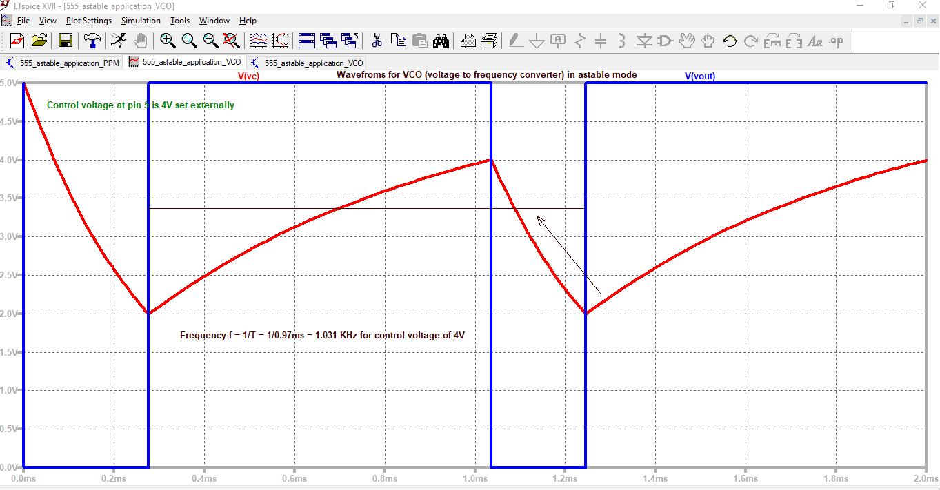
SIMULATION 34.07: Application of Astable Multi-vibrator: Pulse Position modulation circuit
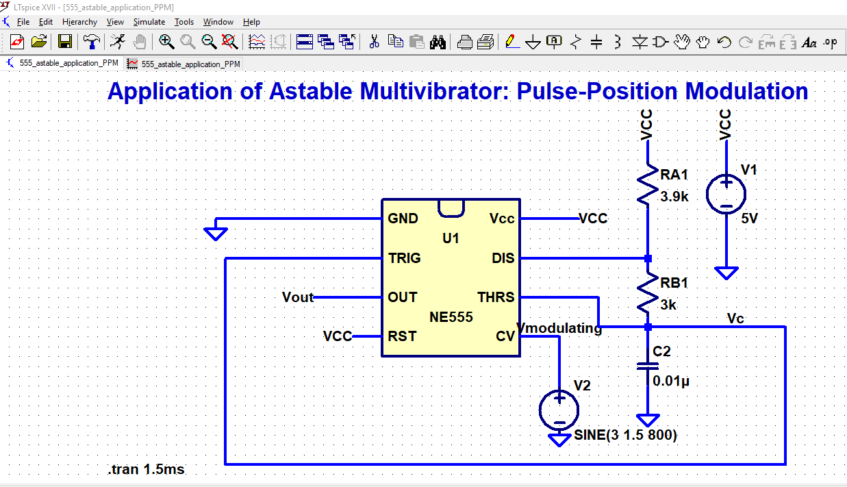
SIMULATION 34.08: Application of Astable Multi-vibrator: Waveform's for Pulse Position modulation
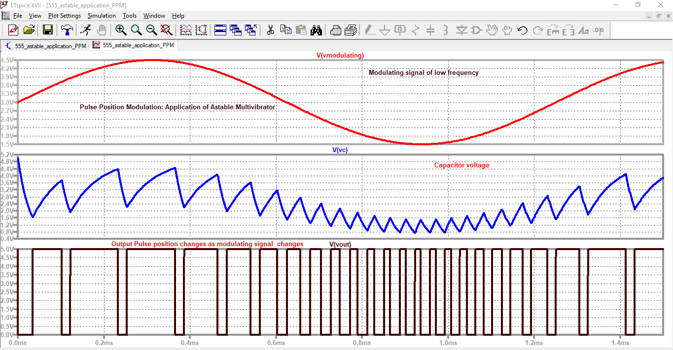
SIMULATION 34.09: Application of Astable Multi-vibrator: Waveform's (combined and plotted together) for Pulse Position modulation
Output pulse position changes as per modulating signal
Output pulse position changes as per modulating signal
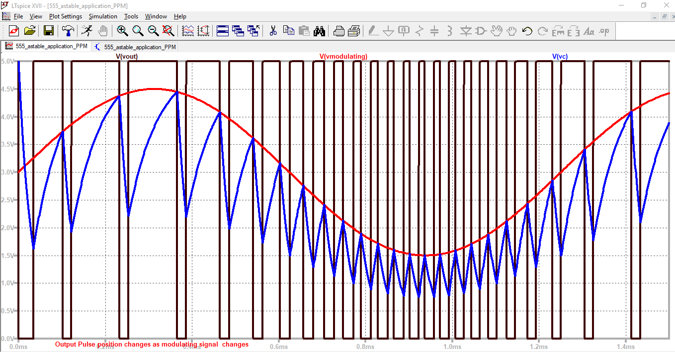
SIMULATION 34.10: Application of Astable Multi-vibrator: Pulse Position modulation circuit
with triangular wave as modulating signal
with triangular wave as modulating signal
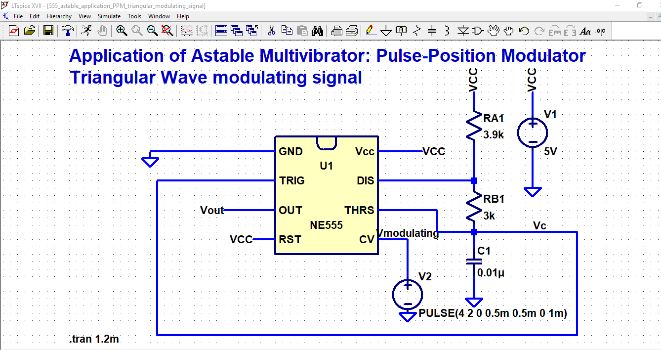
SIMULATION 34.11: Application of Astable Multi-vibrator: Waveform's (combined and plotted together) for Pulse Position modulation
Output pulse position changes as per modulating signal
Output pulse position changes as per modulating signal
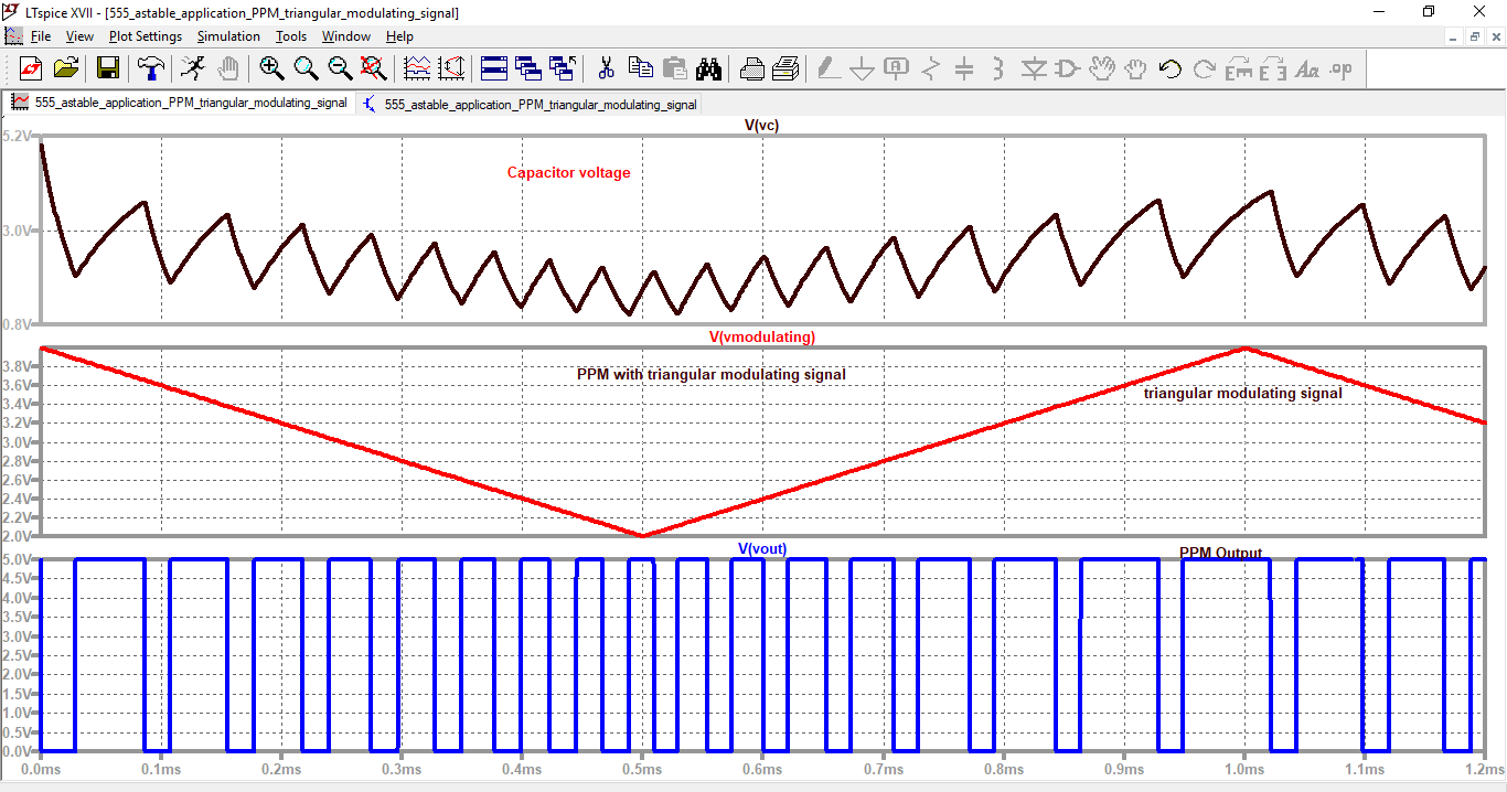
End of Week 12: 03-10-2018 to 04-10-2018
Total no. of Lectures conducted: 02
Total Hours: 02
Activities during week 12:
1) Concepts: Demonstrated in LT Spice schematic and simulation tool
2) Numerical examples: Demonstrated in LT Spice schematic and simulation tool
3) Applications of 555 timer were demonstrated in LT Spice schematic and simulation tool
4) Concept working was explained with the help of numerical examples.
Lecture 35 handout dated 09-10-2018: uploaded on 11/10/2018 by 1:05 am
Topics Covered: Introduction to filters with examples and its simulation in LT Spice, types of filters, Passive 1st order LPF, HPF and BPF circuit and frequency response and its verification in LT Spice simulation and hands-on calculations. Advantages of Active filters and passive filter.
Topics Covered: Introduction to filters with examples and its simulation in LT Spice, types of filters, Passive 1st order LPF, HPF and BPF circuit and frequency response and its verification in LT Spice simulation and hands-on calculations. Advantages of Active filters and passive filter.
| licd_35.pdf |
SIMULATIONS related to lecture 35 are below : 35.01 to 34.06 ( Total 06 images)
SIMULATION 35.01: Passive RC 1st order Low pass filter circuit
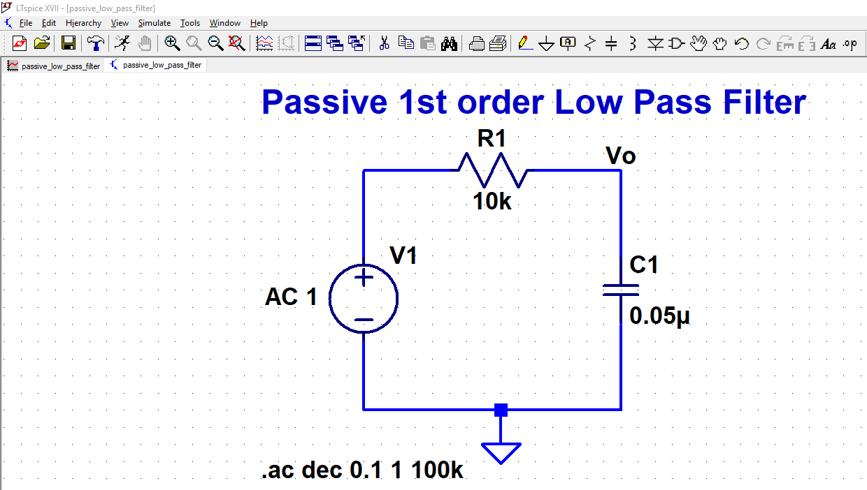
SIMULATION 35.02: Frequency Response of Passive 1st order Low pass filter circuit
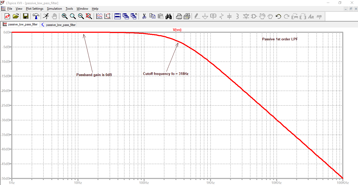
SIMULATION 35.03: Passive RC 1st order High pass filter circuit
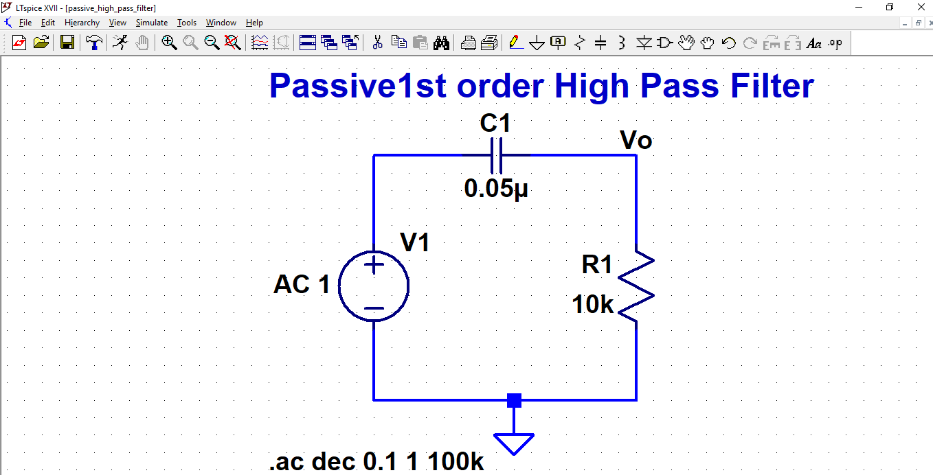
SIMULATION 35.04: Frequency Response of Passive 1st order High pass filter circuit
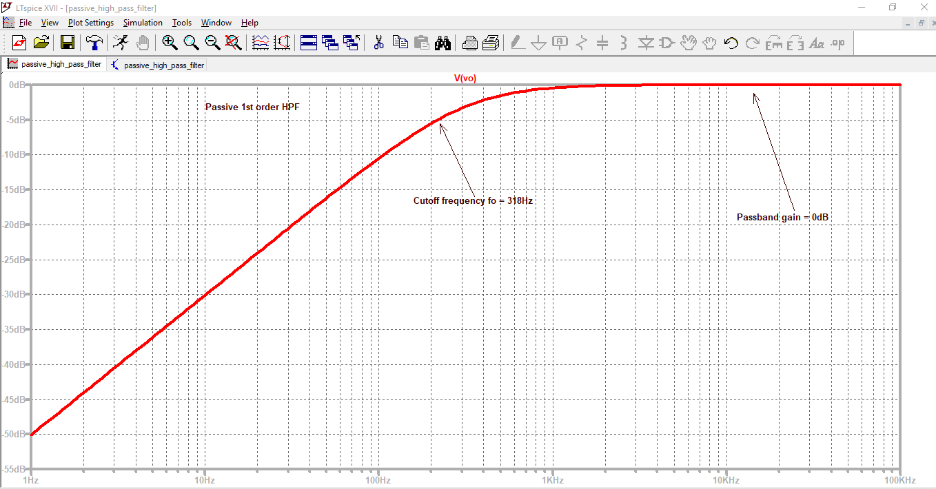
SIMULATION 35.05: Passive RC 1st order Band pass filter circuit
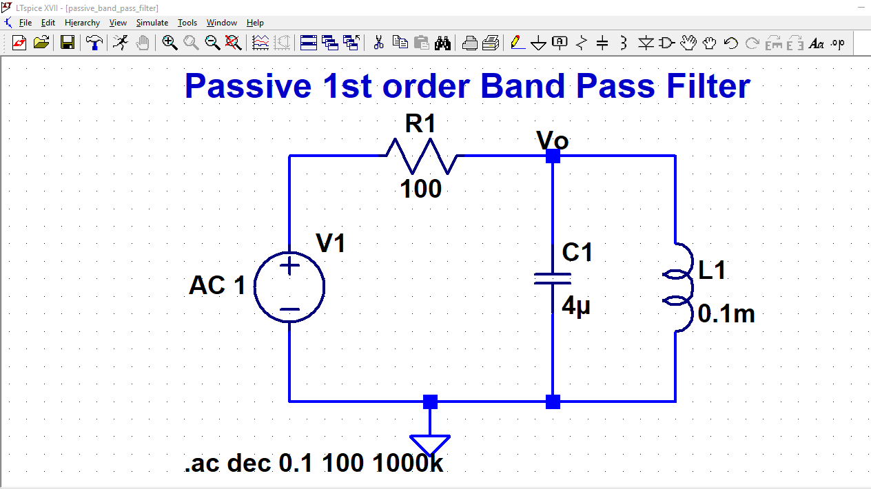
SIMULATION 35.06: Frequency Response of Passive 1st order Band pass filter circuit
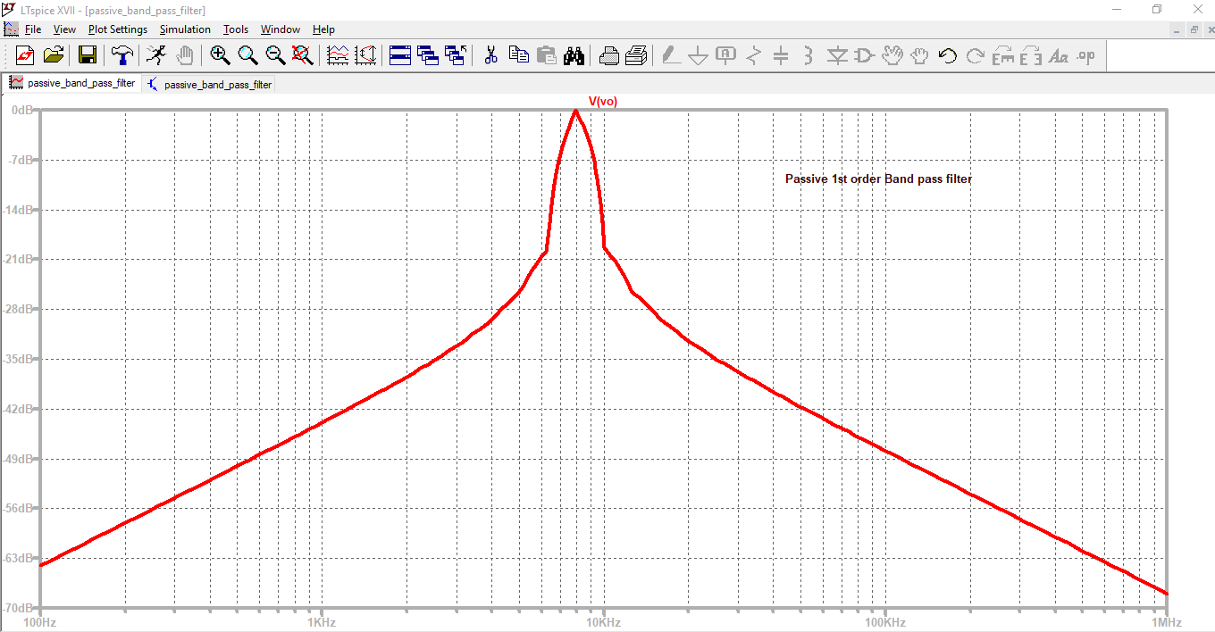
Lecture 36 handout dated 10-10-2018: uploaded on 11/10/2018 by 10:30 am
Topics Covered: Analysis of Active 1st order Low pass filter circuit and explanation of its frequency response and its verification in LT Spice simulation and hands-on calculations in form of numerical. Design of Active 1st order Low pass filter and its verification in LT Spice simulation, missing pulse detector: An application of mono-stable multivibrator using 555 timer
Topics Covered: Analysis of Active 1st order Low pass filter circuit and explanation of its frequency response and its verification in LT Spice simulation and hands-on calculations in form of numerical. Design of Active 1st order Low pass filter and its verification in LT Spice simulation, missing pulse detector: An application of mono-stable multivibrator using 555 timer
| licd_36.pdf |
Video related to lecture 36 is below : 36.01 (Total 1)
Video 36.01 : IITB lecture on Active filters
Start video from beginning and watch it till 14 minutes and 25 seconds
SIMULATIONS related to lecture 36 are below : 36.01 to 36.06 ( Total 06 images)
SIMULATION 36.01: Active 1st order Low pass filter circuit (Numerical 01)
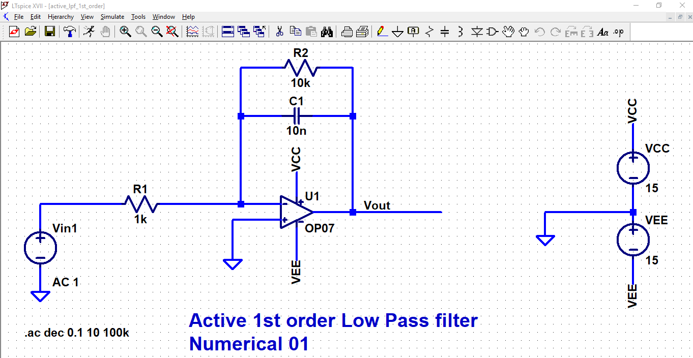
SIMULATION 36.02: Frequency response of 1st order Low pass filter circuit (Numerical 01)
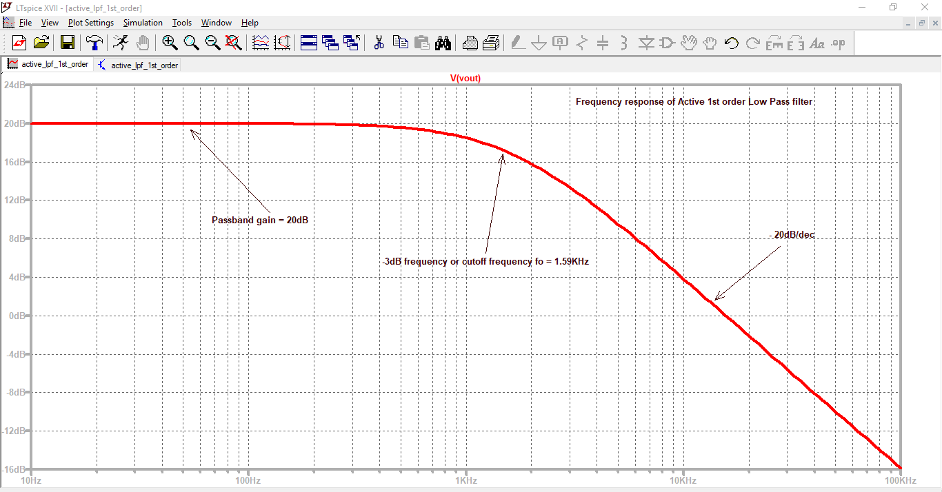
SIMULATION 36.03: Design of 1st order Low pass filter circuit (Design 01)
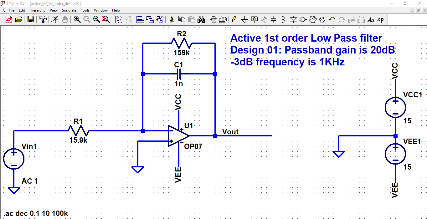
SIMULATION 36.04: Frequency response of designed 1st order Low pass filter (Design 01)
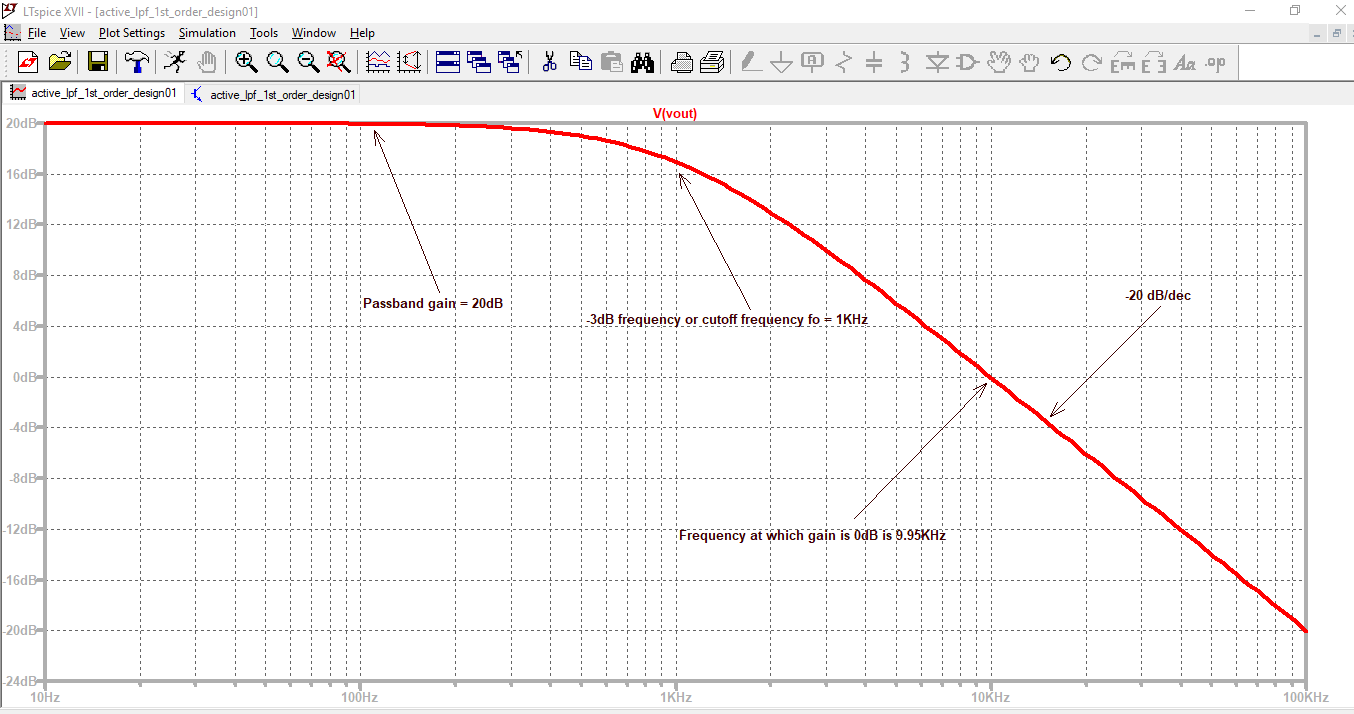
SIMULATION 36.05: Mono-stable multivibrator as Missing Pulse detector using 555 timer
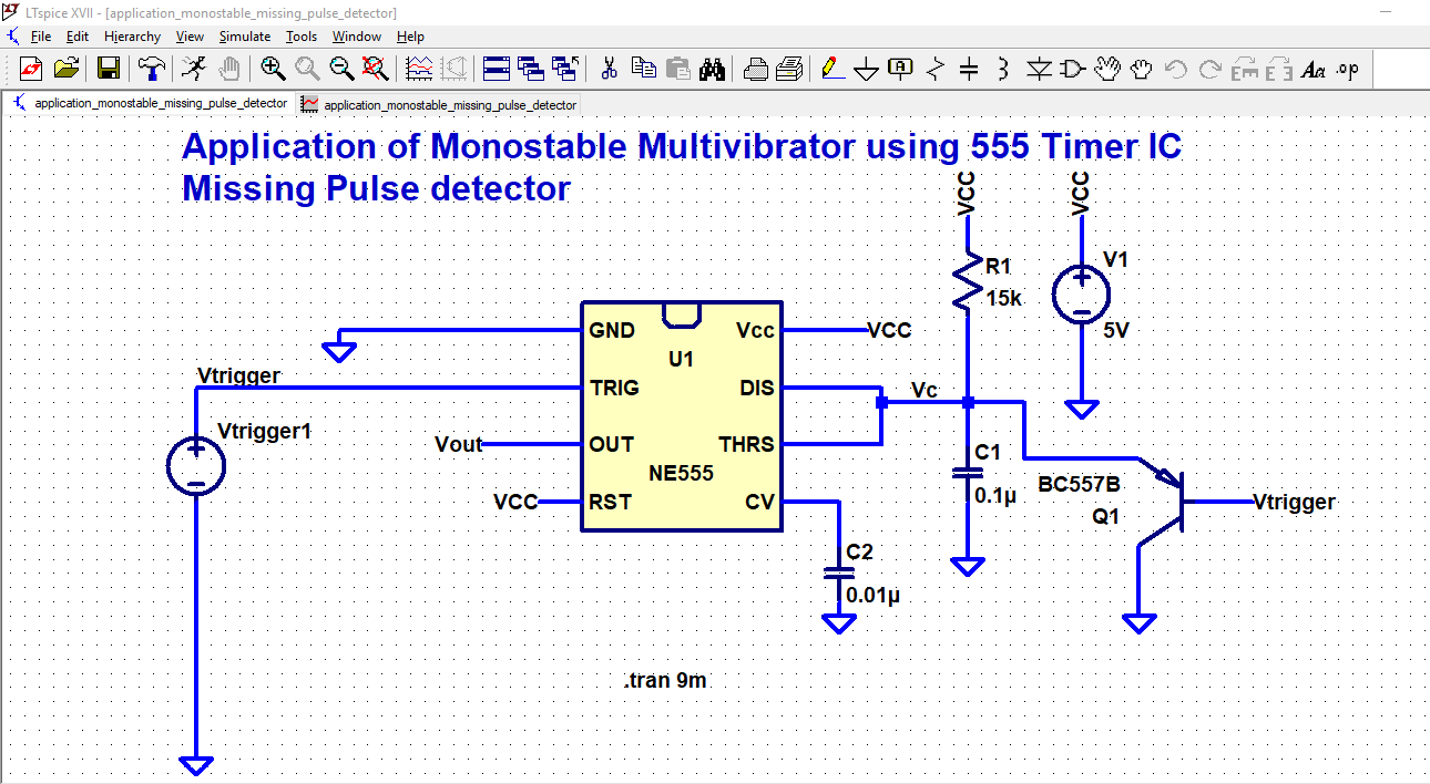
SIMULATION 36.06: Waveform's for Missing pulse detector circuit
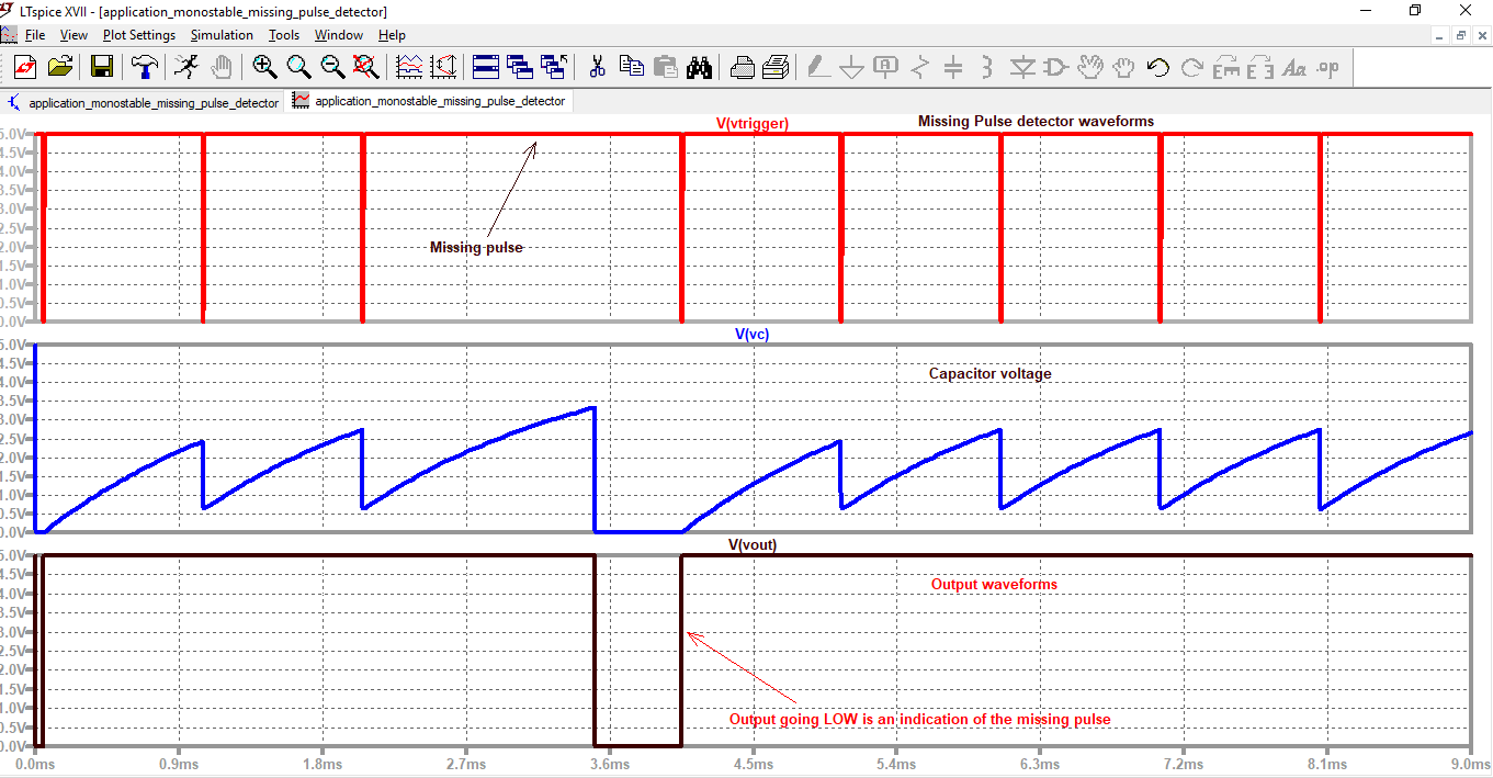
Lecture 37 handout dated 11-10-2018: uploaded on 15/10/2018 by 10:06 am
Topics Covered: Analysis of Active 1st order High pass filter circuit using inverting opamp and explanation of its frequency response and its verification in LT Spice simulation and hands-on calculations in form of numerical. Analysis of Active 1st order High and Low pass filter circuit using opamp in non-inverting mode and explanation of its frequency response and its verification in LT Spice simulation. Design of Active 1st order Low and High pass filter circuit using opamp in non-inverting mode and its verification in LT Spice simulation.
Topics Covered: Analysis of Active 1st order High pass filter circuit using inverting opamp and explanation of its frequency response and its verification in LT Spice simulation and hands-on calculations in form of numerical. Analysis of Active 1st order High and Low pass filter circuit using opamp in non-inverting mode and explanation of its frequency response and its verification in LT Spice simulation. Design of Active 1st order Low and High pass filter circuit using opamp in non-inverting mode and its verification in LT Spice simulation.
| licd_37.pdf |
SIMULATIONS related to lecture 37 are below : 37.01 to 37.06 ( Total 06 images)
SIMULATION 37.01: Numerical 02 on active 1st order High Pass Filter circuit
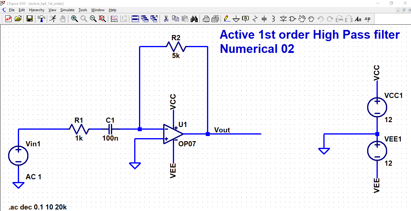
SIMULATION 37.02: Frequency response for Numerical 02 on active 1st order High Pass Filter
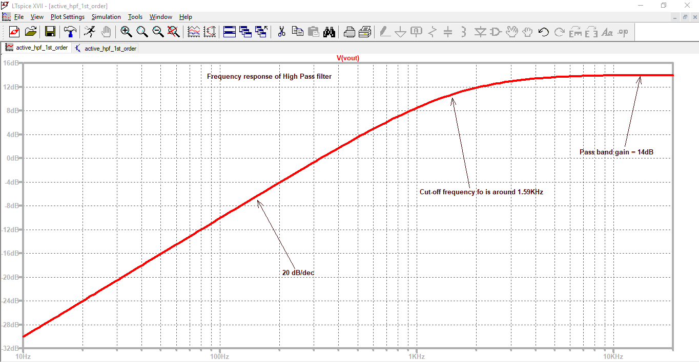
SIMULATION 37.03: Design 02 on active 1st order Low Pass Filter circuit
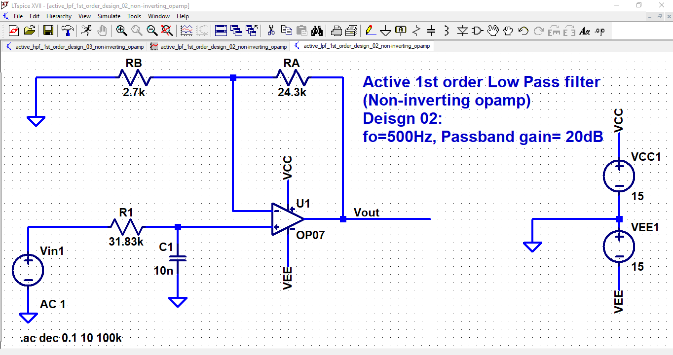
SIMULATION 37.04: Frequency response for design 02 on active 1st order LPF
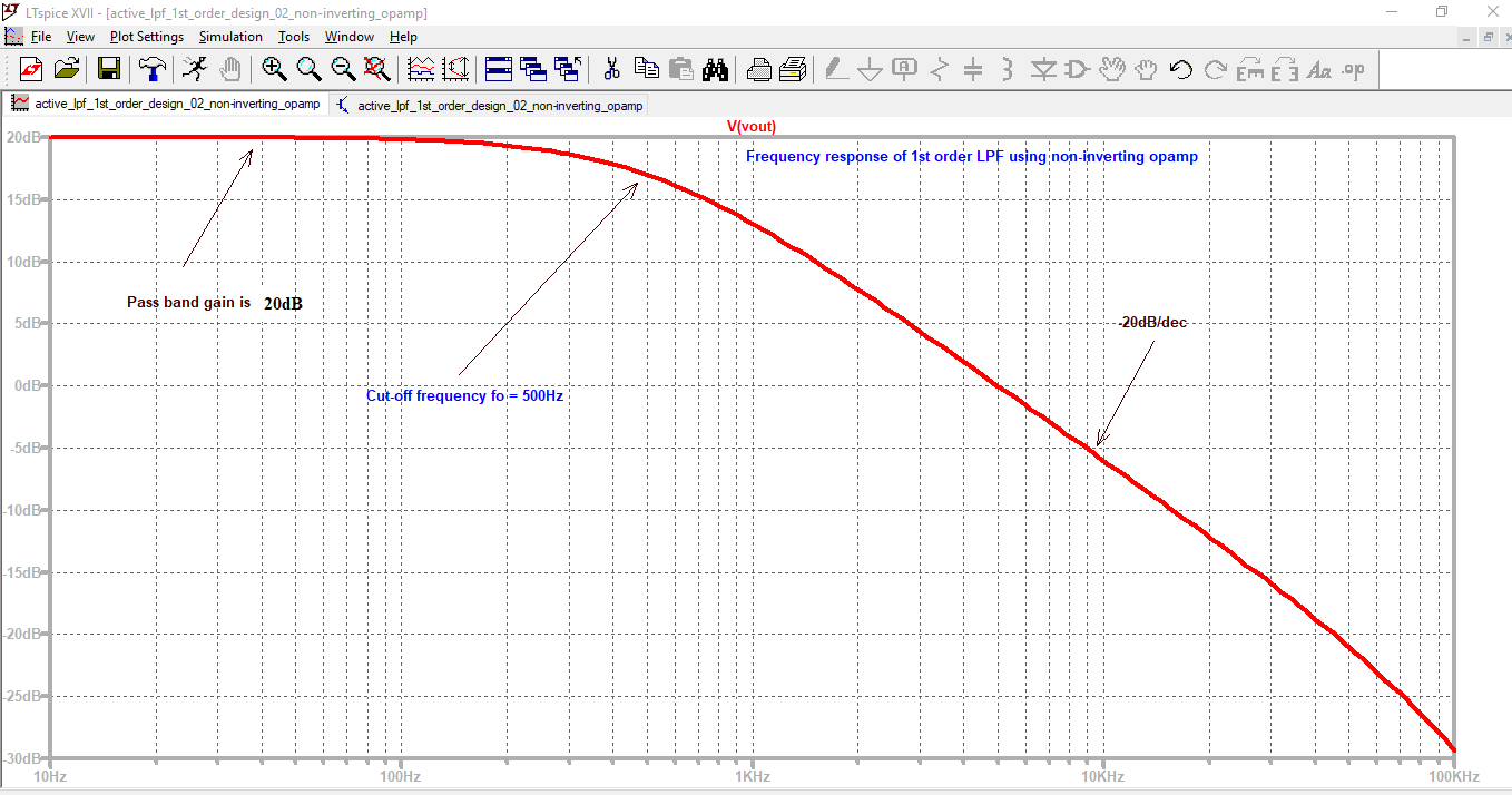
SIMULATION 37.05: Design 03 on active 1st order High Pass Filter circuit
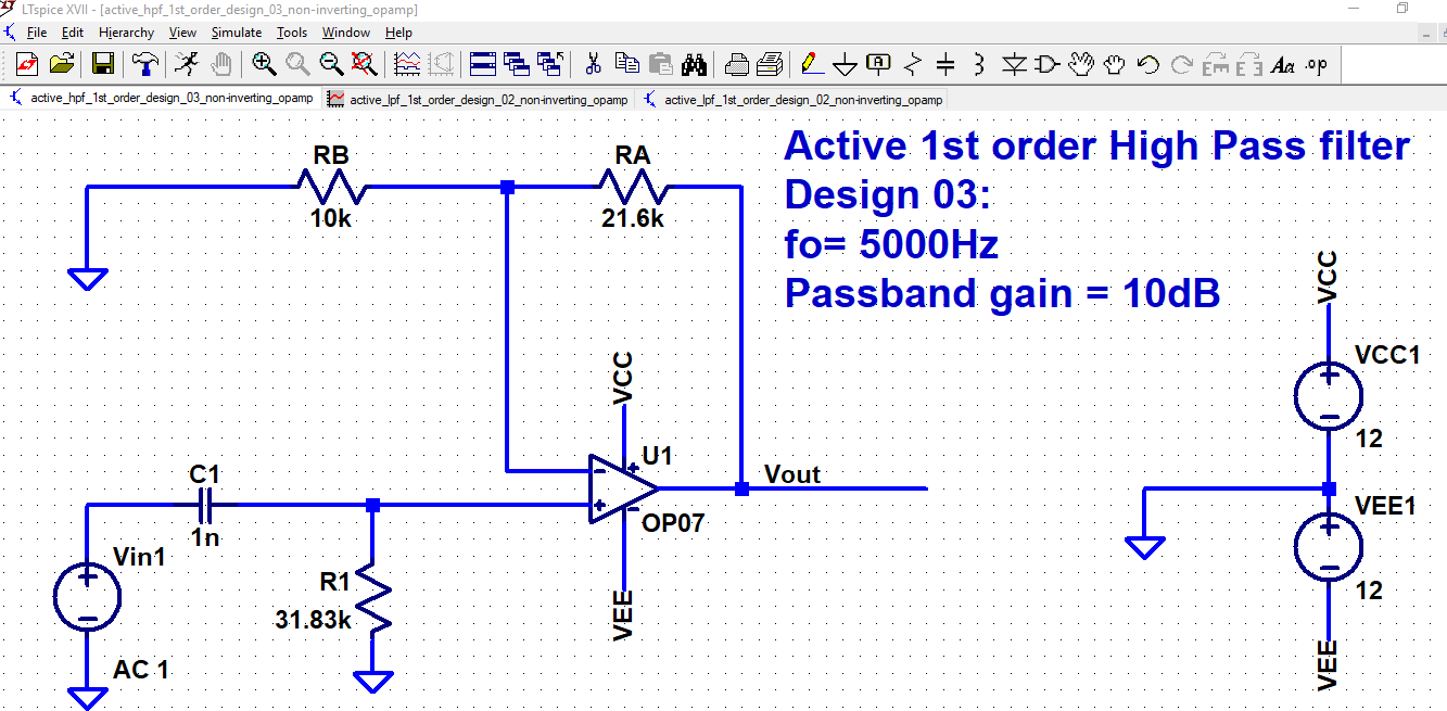
SIMULATION 37.06: Frequency response for design 03 on active 1st order HPF
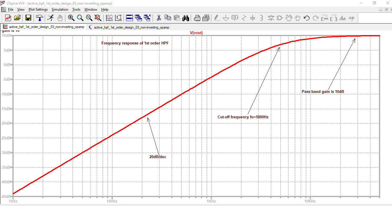
Lecture 38 handout dated 12-10-2018: uploaded on 15-10-2018 by 11:30 am
Topics Covered: Analysis of Active Band pass filter circuit using inverting opamp and explanation of its frequency response and its verification in LT Spice simulation and hands-on calculations in form of numerical. Design of Active Band pass filter circuit using opamp in inverting mode and its verification in LT Spice simulation. Introduction to KRC filters, Working of 2nd order LPF circuit and its frequency response, Generalized derivation for Transfer function for 2nd order systems.
Topics Covered: Analysis of Active Band pass filter circuit using inverting opamp and explanation of its frequency response and its verification in LT Spice simulation and hands-on calculations in form of numerical. Design of Active Band pass filter circuit using opamp in inverting mode and its verification in LT Spice simulation. Introduction to KRC filters, Working of 2nd order LPF circuit and its frequency response, Generalized derivation for Transfer function for 2nd order systems.
| licd_38.pdf |
SIMULATIONS related to lecture 38 are below : 38.01 to 38.04 ( Total 04 images)
SIMULATION 38.01: Numerical on Active Band Pass filter circuit
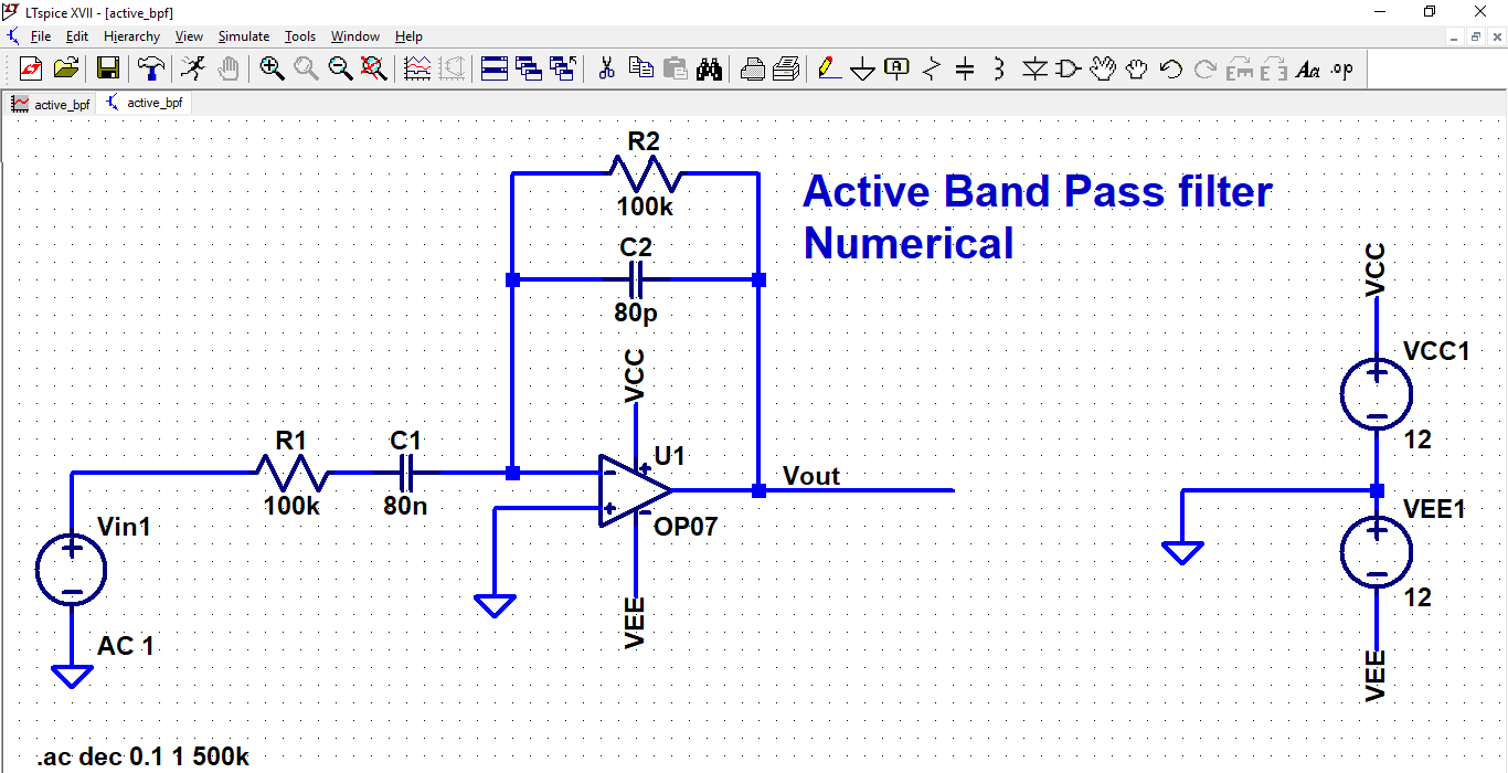
SIMULATION 38.02: Frequency response of Active Band Pass filter circuit
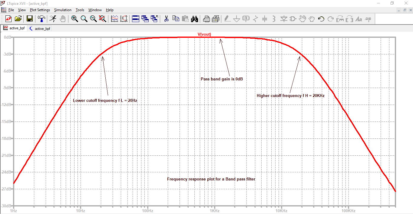
SIMULATION 38.03: Designed Active Band Pass filter circuit
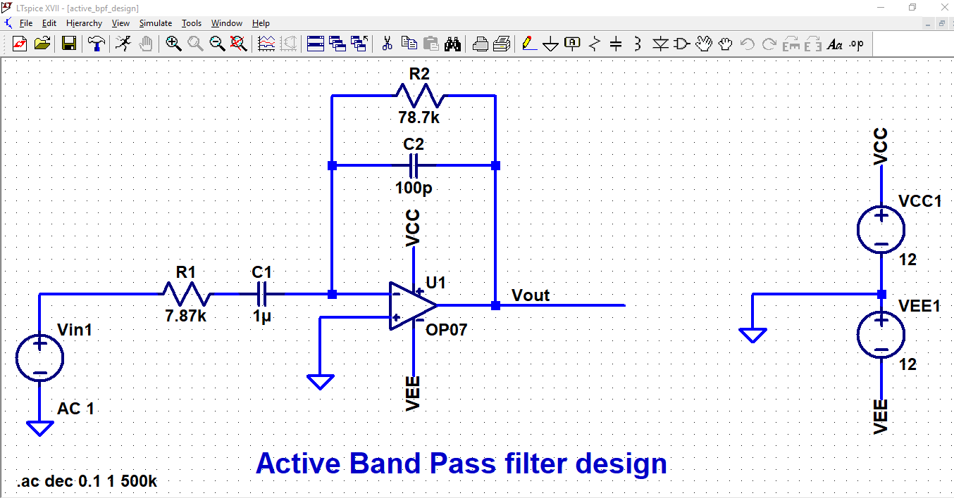
SIMULATION 38.04: Frequency response for designed Active Band Pass filter circuit
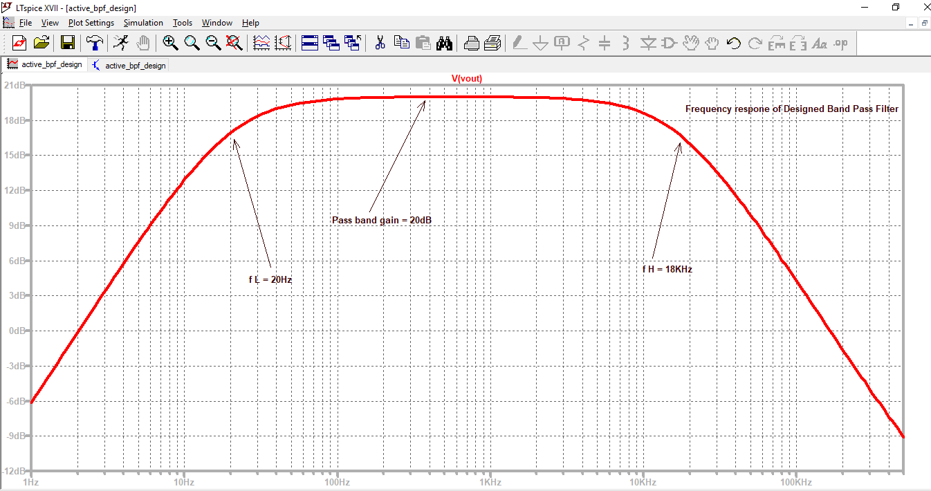
End of Week 13: 09-10-2018 to 12-10-2018
Total no. of Lectures conducted: 04
Total Hours: 04
Activities during week 13:
1) Concepts: Demonstrated in LT Spice schematic and simulation tool
2) Numerical and design examples: Demonstrated in LT Spice schematic and simulation tool
3) Concept working was explained with the help of numerical examples.
4) Many topics during the course of the week 13, were covered using traditional approach
Lecture 39 handout dated 17-10-2018: uploaded on 18-10-2018 by 7:22 pm
Topics Covered: Analysis of 2nd order LPF circuit and its frequency response, generalized derivation for Transfer function, fo and quality factor for 2nd order LPF, Design of 2nd order KRC Low pass filter circuit using equal-component & unity-gain design and its verification in LT Spice simulation.
Topics not covered: Design of 2nd order KRC Butterworth Low pass filter circuit using equal-component and its verification in LT Spice simulation
| licd_39.pdf |
SIMULATIONS related to lecture 39 are below : 39.01 to 39.06 ( Total 06 images)
SIMULATION 39.01: Designed 2nd order KRC LPF circuit using equal component design
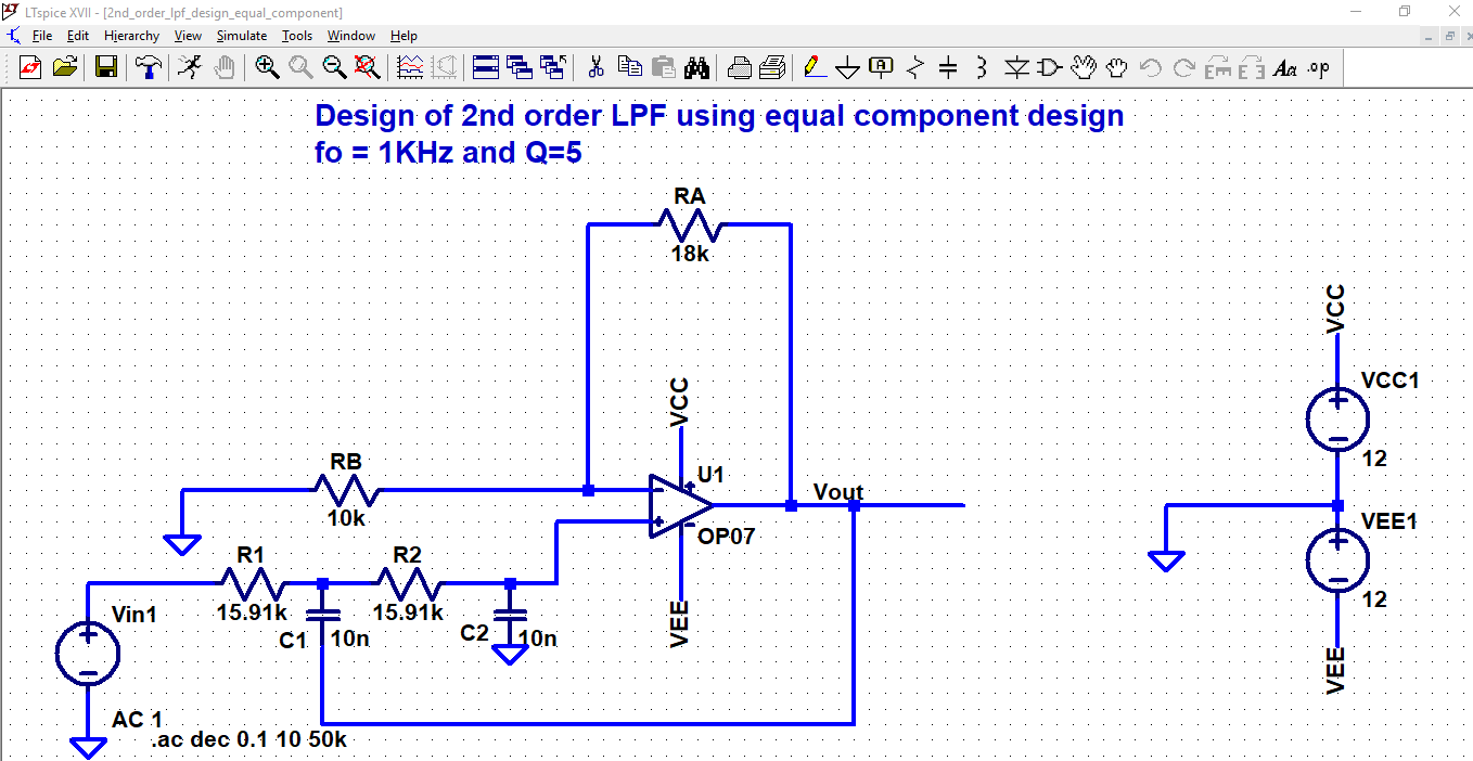
SIMULATION 39.02: Frequency response of 2nd order KRC LPF circuit using equal component design
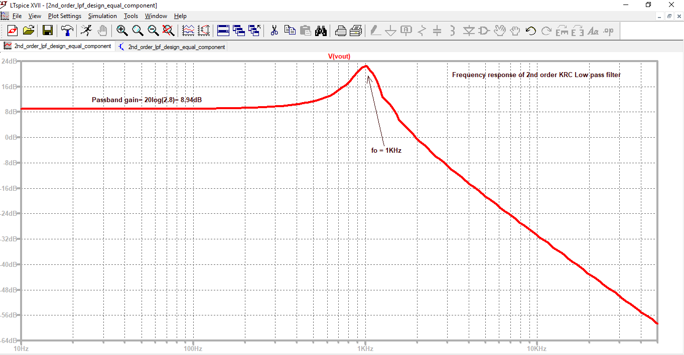
SIMULATION 39.03: Designed 2nd order KRC LPF circuit using unity gain design
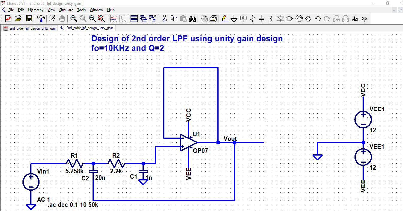
SIMULATION 39.04: Frequency response of Designed 2nd order KRC LPF circuit using unity gain design
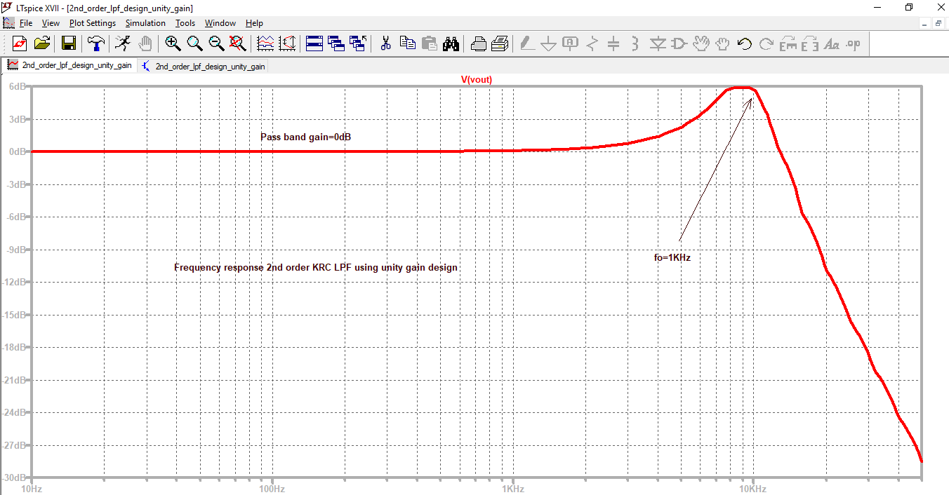
SIMULATION 39.05: Design of 2nd order KRC Butterworth LPF circuit using equal component design
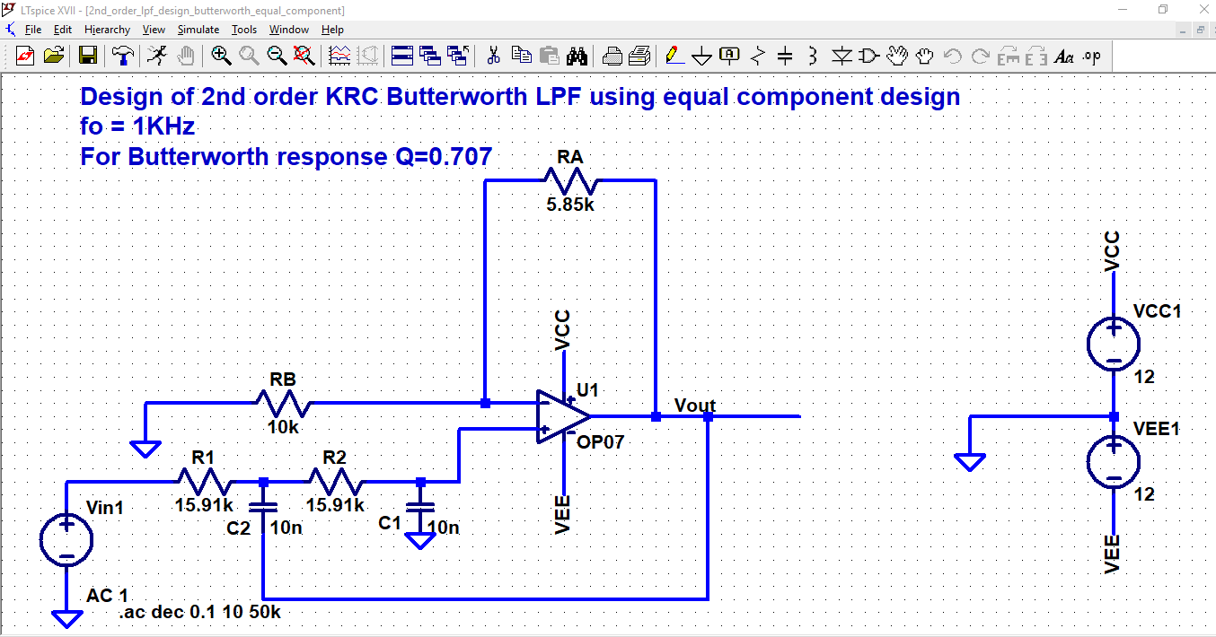
SIMULATION 39.06: Frequency response of 2nd order KRC Butterworth LPF circuit using equal component design
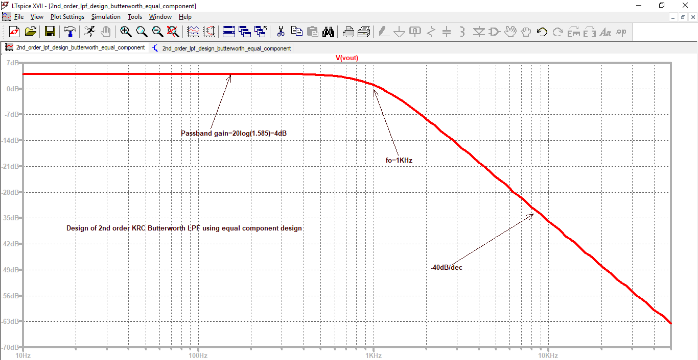
Lecture 40 handout dated 17-10-2018: uploaded on 18-10-2018 by 7:23 pm
Topics Covered: Impact of Quality factor (Q) on 2nd order LPF frequency response, Analysis of 2nd order HPF circuit and its frequency response, generalized derivation for Transfer function, fo and quality factor for 2nd order HPF, Design of 2nd order KRC high pass filter circuit using equal-component design and its verification in LT Spice simulation. Introduction to Band pass filters.
Topics Covered: Impact of Quality factor (Q) on 2nd order LPF frequency response, Analysis of 2nd order HPF circuit and its frequency response, generalized derivation for Transfer function, fo and quality factor for 2nd order HPF, Design of 2nd order KRC high pass filter circuit using equal-component design and its verification in LT Spice simulation. Introduction to Band pass filters.
| licd_40.pdf |
| standard_second_order_transfer_functions.pdf |
SIMULATIONS related to lecture 40 are below : 40.01 to 40.04 ( Total 04 images)
SIMULATIONS related to lecture 40 are below : 40.01 to 40.04 ( Total 04 images)
SIMULATION 40.01: Impact of different values of Q on 2nd order KRC LPF circuits
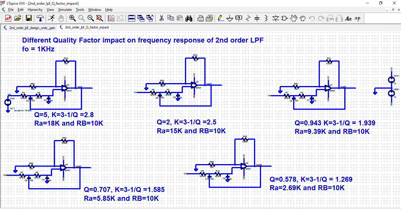
SIMULATION 40.02: Frequency responses of 2nd order KRC LPF for different values of Q
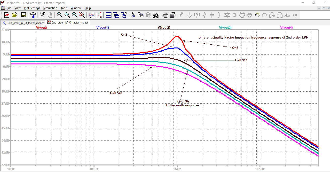
SIMULATION 40.03: Designed 2nd order KRC HPF circuit using equal component design
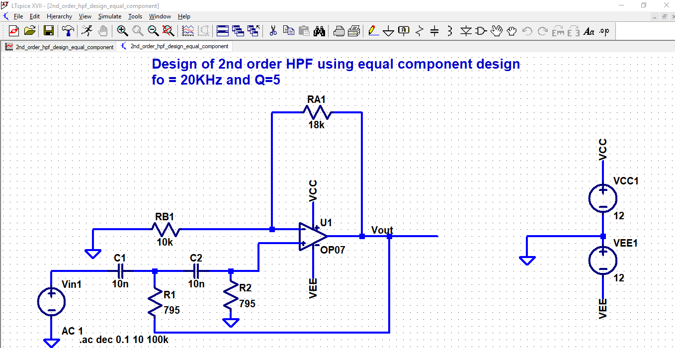
SIMULATION 40.04: Frequency response of Designed 2nd order KRC LPF using equal component design
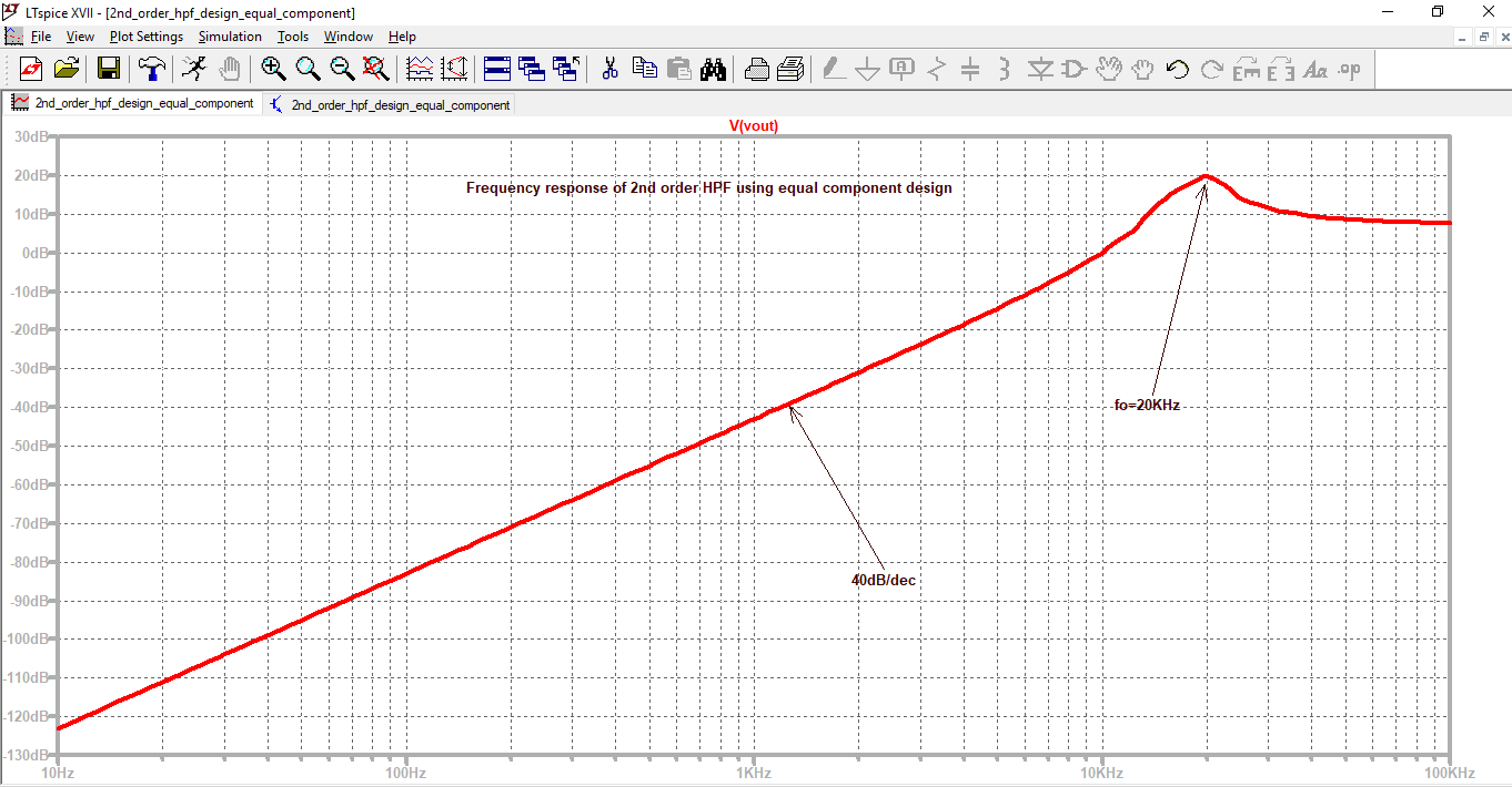
Lecture 41 handout dated 19-10-2018: uploaded on 22-10-2018 by 12:58 am
Topics Covered: Analysis of 2nd order Band pass filter circuit and its frequency response, generalized derivation for Transfer function, fo and quality factor for 2nd order BPF, Design of 2nd order KRC band pass filter circuit using equal-component design and its verification in LT Spice simulation. Introduction to Band reject filter, its working and frequency response, Design of Notch (Band reject) filter and its verification in LT Spice simulation
Topics Covered: Analysis of 2nd order Band pass filter circuit and its frequency response, generalized derivation for Transfer function, fo and quality factor for 2nd order BPF, Design of 2nd order KRC band pass filter circuit using equal-component design and its verification in LT Spice simulation. Introduction to Band reject filter, its working and frequency response, Design of Notch (Band reject) filter and its verification in LT Spice simulation
| licd_41.pdf |
SIMULATIONS related to lecture 41 are below : 41.01 to 41.04 ( Total 04 images)
SIMULATIONS related to lecture 41 are below : 41.01 to 41.04 ( Total 04 images)
SIMULATION 41.01: Designed 2nd order KRC BPF circuit using equal component design
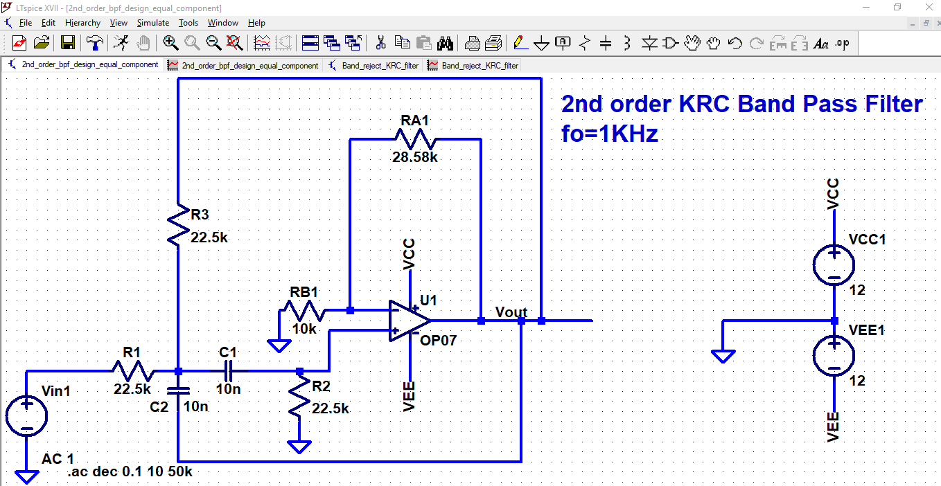
SIMULATION 41.02: Frequency response of Designed 2nd order KRC BPF
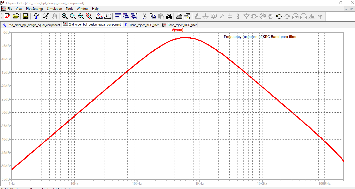
SIMULATION 41.03: Designed Notch filter for 60Hz
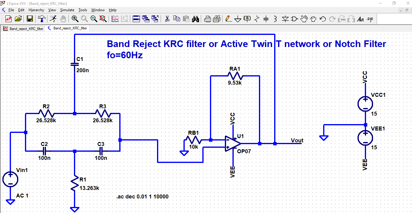
SIMULATION 41.04: Frequency response of Designed Notch filter
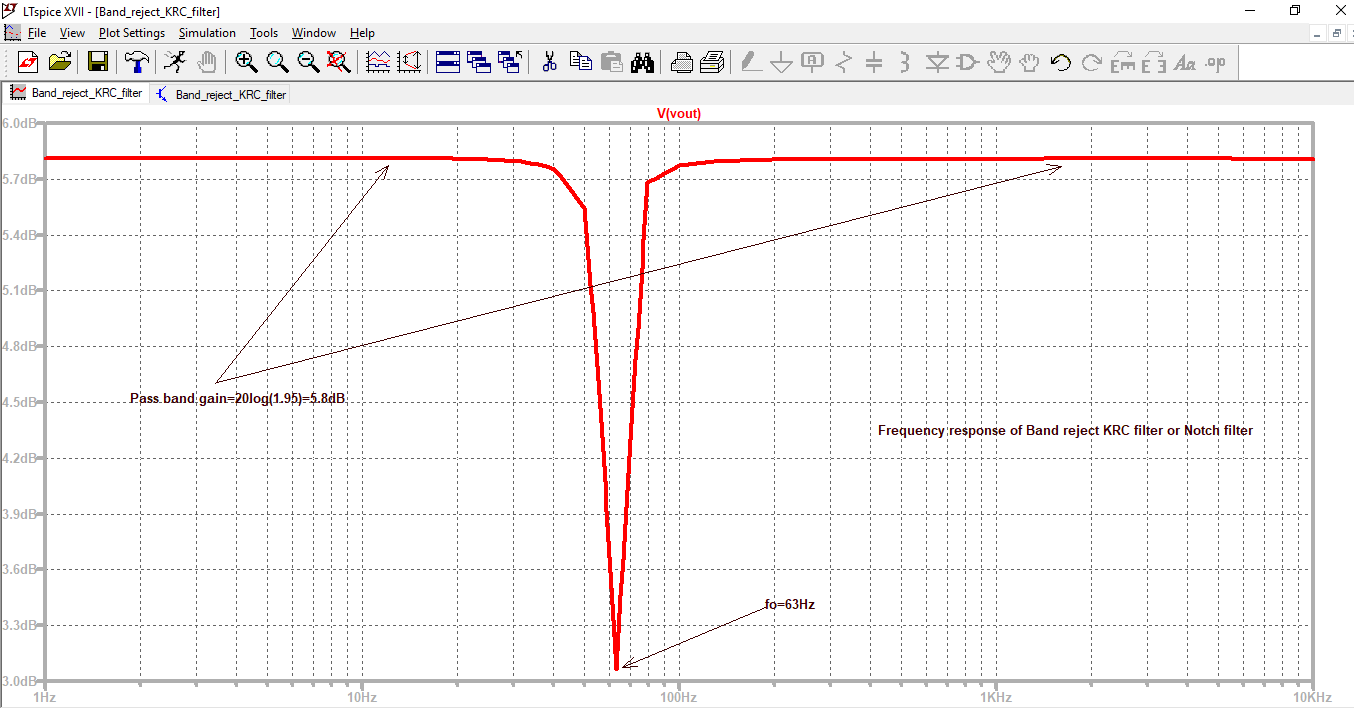
End of Week 14: 17-10-2018 to 19-10-2018
Total no. of Lectures conducted: 03
Total Hours: 03
Activities during week 14:
1) Concepts: Demonstrated in LT Spice schematic and simulation tool
2) Numerical examples: Demonstrated in LT Spice schematic and simulation tool
3) Filter circuits were demonstrated in LT Spice schematic and simulation tool
4) Concept working was explained with the help of numerical examples.
Lecture 42 handout dated 30-10-2018: uploaded on 15/11/2018 by 10:23 pm
Topics Covered: Analysis of Multiple feedback Band pass filter circuit and its frequency response, derivation for Transfer function, fo and quality factor for multiple feedback BPF, Design of multiple feedback band pass filter circuit and its verification in LT Spice simulation. Introduction to Multiple feedback Low pass filter and its frequency response demonstration in LT Spice simulation
Topics Covered: Analysis of Multiple feedback Band pass filter circuit and its frequency response, derivation for Transfer function, fo and quality factor for multiple feedback BPF, Design of multiple feedback band pass filter circuit and its verification in LT Spice simulation. Introduction to Multiple feedback Low pass filter and its frequency response demonstration in LT Spice simulation
| licd_42.pdf |
SIMULATIONS related to lecture 42 are below : 42.01 to 42.04 ( Total 04 images)
SIMULATION 42.01: Designed multiple feedback Band Pass filter circuit
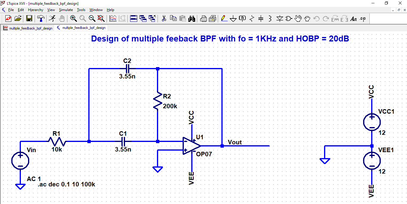
SIMULATION 42.02: Frequency response of Designed multiple feedback Band Pass filter circuit
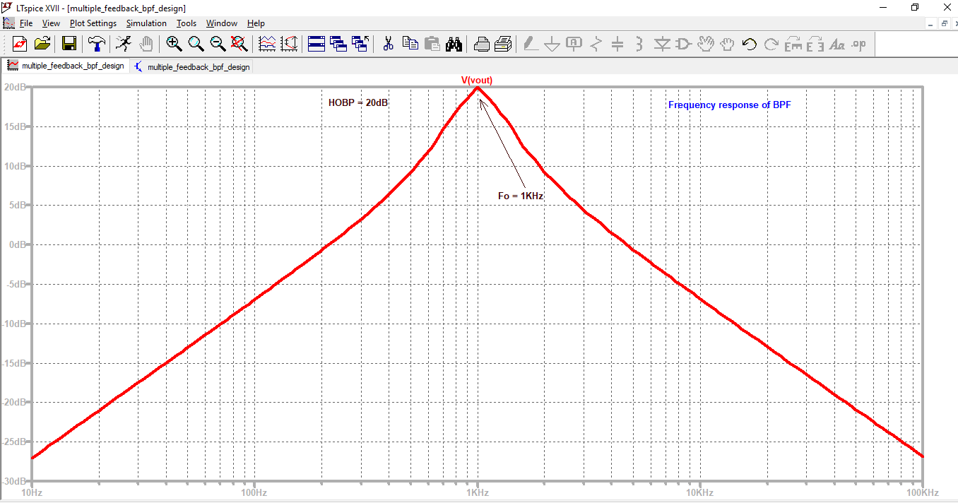
SIMULATION 42.03: Demonstration of Multiple feedback LPF circuit ( Circuit taken from Sergio Franco textbook)
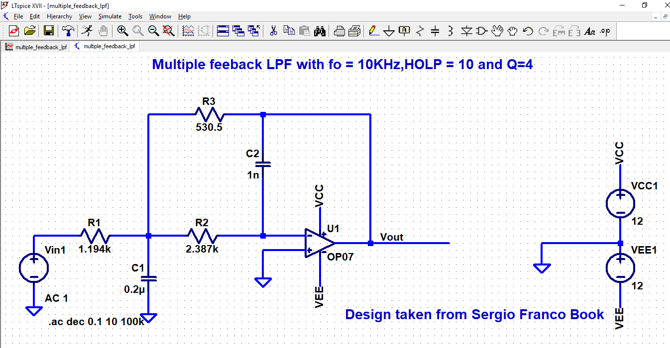
SIMULATION 42.04: Frequency response of Multiple feedback LPF
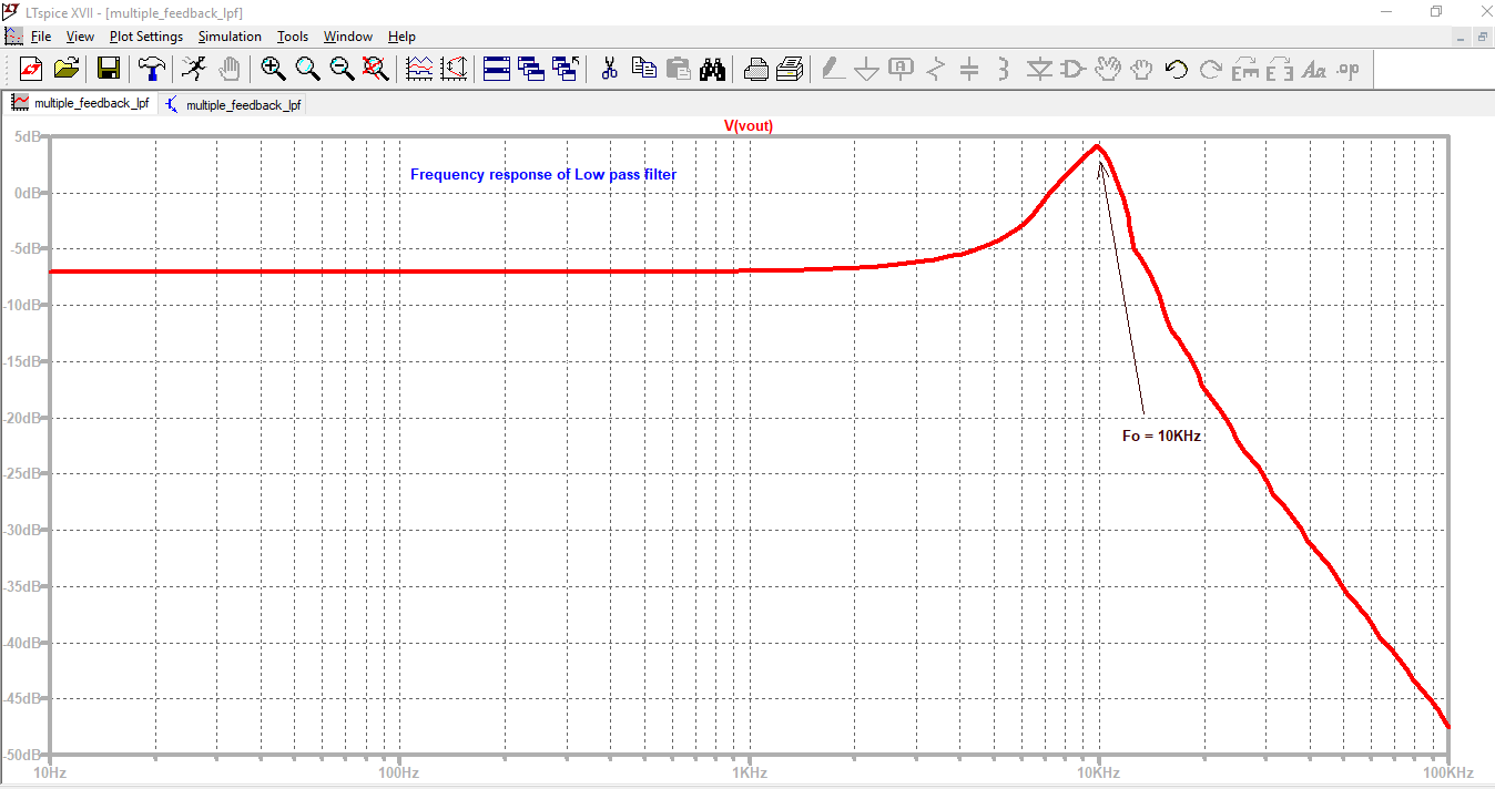
Lecture 43 handout dated 31-10-2018: uploaded on 17/11/2018 by 11:50 pm
Topics Covered: Introduction to Voltage regulators, classification of regulators, Working of Series/ linear voltage regulator, IC voltage regulator features, Fixed voltage regulators ( 78XX and 79XX series), its pin-out, connection diagram and its characteristics, line and load regulation concept, Fixed voltage regulator (e.g 7805) as a current source: Analysis and design
Topics Covered: Introduction to Voltage regulators, classification of regulators, Working of Series/ linear voltage regulator, IC voltage regulator features, Fixed voltage regulators ( 78XX and 79XX series), its pin-out, connection diagram and its characteristics, line and load regulation concept, Fixed voltage regulator (e.g 7805) as a current source: Analysis and design
| licd_43.pdf |
Lecture 44 handout dated 2-11-2018: uploaded on 17/11/2018 by 11:50 pm
Topics Covered: Fixed voltage regulators (e.g 7805) as adjustable voltage regulators: Analysis and design, Boosting the output current of a Fixed voltage regulator ( e.g 7805) using external power transistor, Design of Dual DC power supply ( +15V-0V-(-15V)) using IC 7815 and IC 7915
Topics Covered: Fixed voltage regulators (e.g 7805) as adjustable voltage regulators: Analysis and design, Boosting the output current of a Fixed voltage regulator ( e.g 7805) using external power transistor, Design of Dual DC power supply ( +15V-0V-(-15V)) using IC 7815 and IC 7915
| licd_44.pdf |
Diwali Break from 6/11/2018 to 11/11/2018
LICD IA 1 scores dated 8-9-2018
| licd_ia1_scores.pdf |
Announcement as on 11/11/2018
Extra Lecture of LICD and paper distribution on 13/11/2018
Schedule for the day ( 13/11/2018)
Midterm 1 and 2 paper distribution : 12 to 12:45 pm
LICD CA sheet Signature : 1:15 to 1:45 pm ( Attendance compulsory for all students : A division)
CA sheet signature ( contains information on Midterm 1 and 2 marks plus IA 1 marks and IA 2 marks)
LICD Lecture from 2 pm to 4:45 pm
Lecture 45,46,47 handout dated 13-11-2018: Uploaded on 21/11/2018 by 9:30 pm (Lec 45 & 46 only)
Remaining lec 47 will upload by 23-11-2018 ( also, a miscellaneous numerical's handout will also be uploaded on 23-11-2018 by 5pm)
LAST LICD LECTURE (3.5 hours long)
Topics Covered: 3 terminal Adjustable voltage regulators (LM 317): Its pinout, connection diagram, protection circuitry, and design.
General purpose regulator IC 723: Its features, functional block diagram, pinout. IC723 as a low voltage low current regulator: Working and analysis, its current limit protection, IC 723 as a high voltage regulator: working and analysis, Design numerical's on IC 723 as Low voltage low current regulator, IC 723 as high voltage low current regulator, and IC 723 as low voltage high current regulator.
Compensation techniques for Input bias currents, input offset current, input offset voltage and output offset voltage, Numerical on Input bias currents, input offset current, input offset voltage and output offset voltage for opamp in inverting or non-inverting configuration.
Concept of Slew rate: Its definition, mathematical representation, its causes and its effect on Frequency of opamp, Two different variety of numerical based on Slew rate.
| licd_45.pdf |
| licd_46.pdf |
| licd_47.pdf |
| licd_miscellaneous_numerical.pdf |
Summary of LICD lectures:
Duration: 17/7/2018 to 13/11/2018
Total Lectures conducted: 47
Syllabus Coverage: 85 %
Duration: 17/7/2018 to 13/11/2018
Total Lectures conducted: 47
Syllabus Coverage: 85 %
LICD Practical's Videos
Data Sheets and 555 timer cartoons:
| ua741.pdf |
| op07.pdf |
| ad620.pdf |
| ne555.pdf |
| signetics555timer.pdf |