"An investment in knowledge pays the best interest"
Course Objectives:
1. To deliver the knowledge about physics of basic semiconductor devices and circuits.
2. To enhance comprehension capabilities of students through understanding of electronic devices and circuits
3. To introduce and motivate students to the use of advanced microelectronic devices
4. To analyze and design electronic circuits using semiconductor devices.
Course Outcomes:
1. Students will be able to explain working of semiconductor devices.
2. Students will be able to analyze characteristics of semiconductor devices.
3. Students will be able to perform DC and AC analysis of Electronics circuits.
4. Students will be able to compare various biasing circuits as well as various configurations of BJT,JFET and MOSFETs.
5. Students will be able to select best circuit for the given specifications/application.
6. Students will be able to design electronics circuits for given specifications.
EDC 1 Course Syllabus
Module 01 : PN junction Diode Analysis and applications.
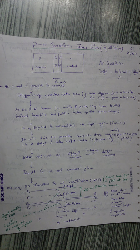
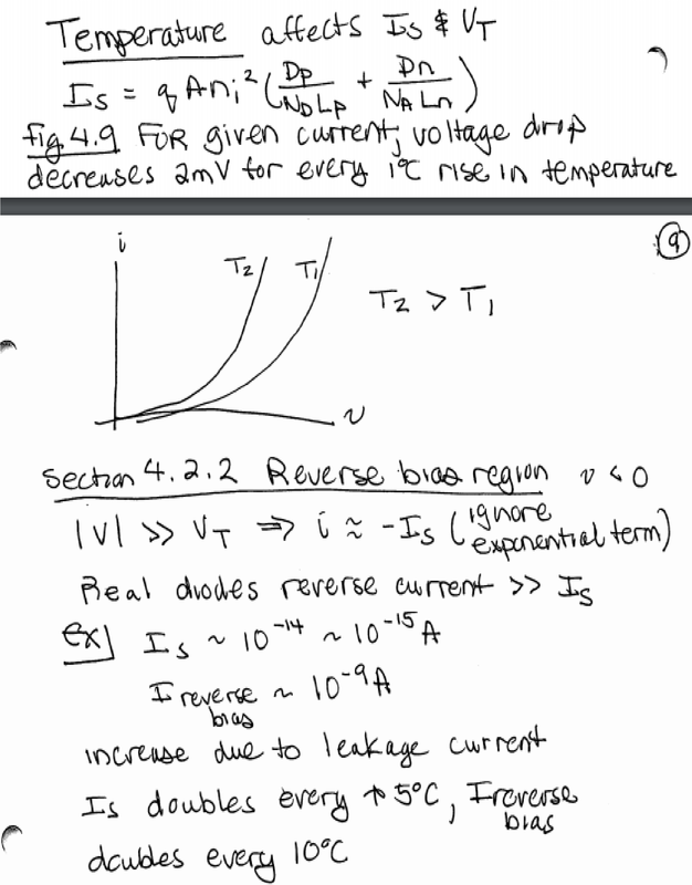
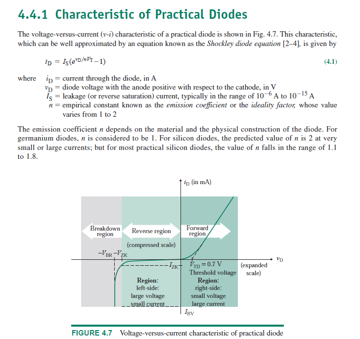
1.1 PN junction Diode: Basic Structure, Energy Band Diagrams, Zero Applied Bias, Forward bias, Reverse bias, PN junction current, drift and diffusion current, junction capacitance, , DC load line, small signal model , Applied Bias, Reverse Applied Bias, temperature effects.
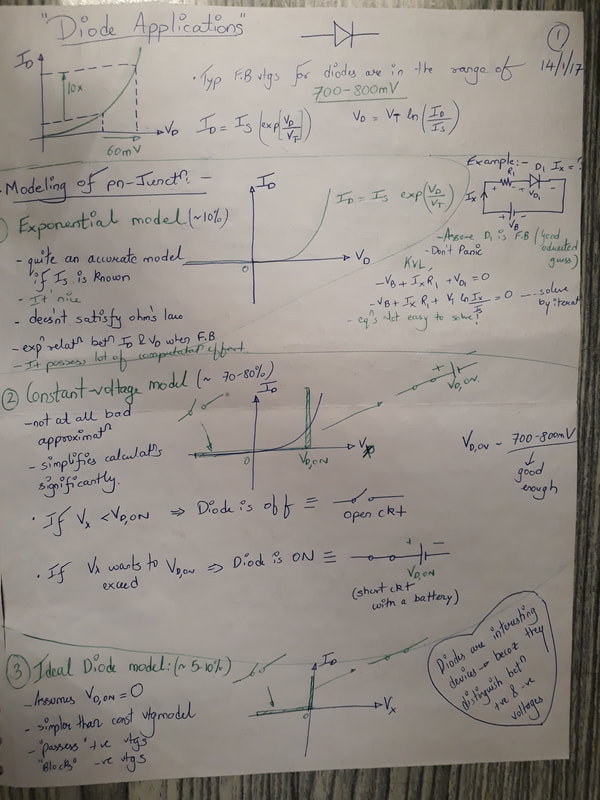
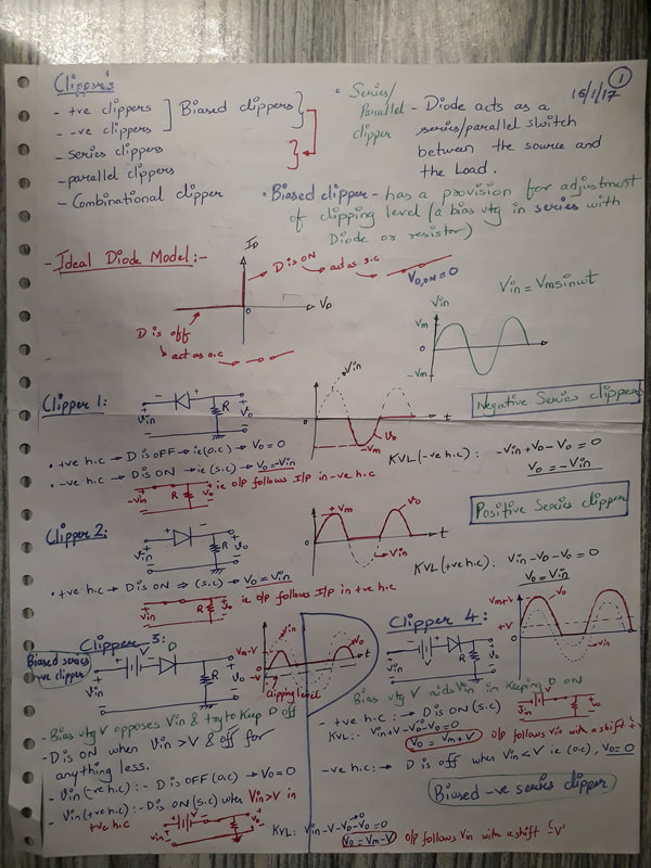
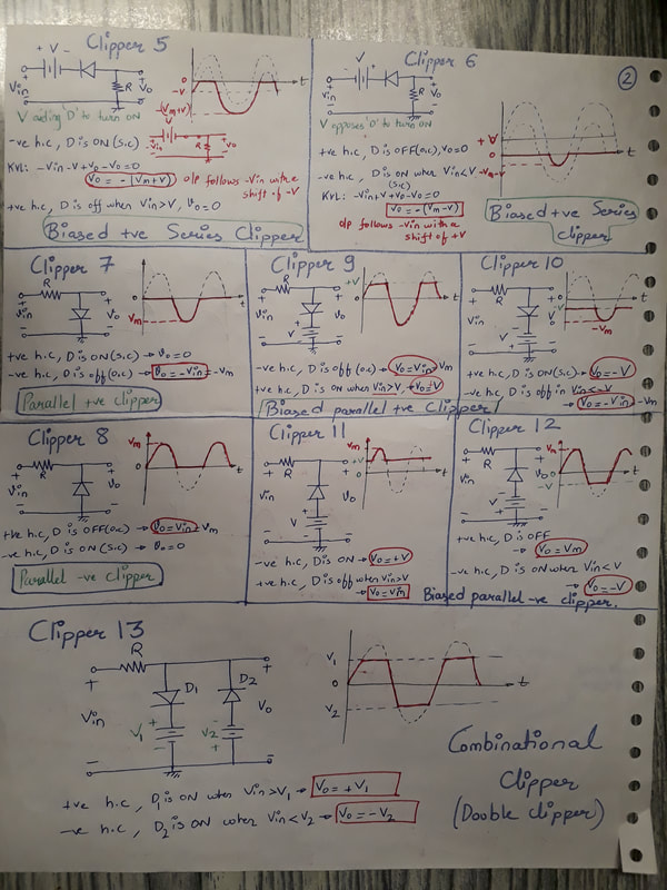
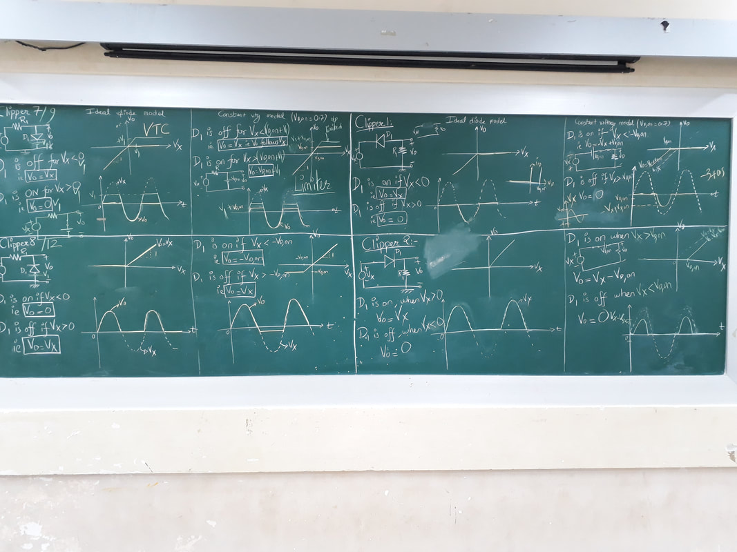
1.2 Clippers and Clampers
Module 02 : Bipolar Junction Transistor
2.1 BJT operations, voltages and currents, BJT characteristics ( CE, CB, CC configurations) , early effect
2.2 DC Circuit Analysis: DC load line and region of Operation, Common Bipolar Transistor Configurations, biasing circuits, bias stability and compensation, analysis and design of biasing circuits.
2.3 AC Analysis of BJT Amplifiers : AC load line, small signal models ( h-parameter model, re model, Hybrid-pi model), graphical analysis, ac equivalent circuits and analysis to obtain voltage gain, current gain, input impedance, output impedance of CE,CB and CC amplifiers
Module 03 : Field Effect Devices
3.1 JFET: Construction, operation and characteristics. MOSFET: Construction, operation and characteristics of D-MOSFET and E-MOSFET.
3.2 DC Circuit Analysis : DC load line and region of operation, Common-MOSFETs configurations, Analysis and Design of Biasing Circuits
3.3 AC Analysis: AC load line, Small-Signal model of MOSFET and its equivalent Circuit, Small-Signal Analysis MOSFET Amplifiers ( Common-Source, Source Follower, Common Gate)
Module 04 : Special semiconductor devices – I
4.1 Construction, working and characteristics of : Zener diode, Schottkey diode, Varactor diode, Tunnel diode, Solar Cells, Photodiodes, LEDs
Module 05 : Rectifiers and Regulators
5.1 Rectifiers: working and analysis of Half wave, Full wave and Bridge
5.2 Filters: C,L,LC, pi
5.3 Regulators: Zener shunt regulator, Series and shunt regulator using single transistor and Zener
Module 06 : Design of electronic circuits
6.1 Design of single stage CE amplifier
6.2 Design of single stage CS MOSFET amplifier
6.3 Design of full wave rectifier with LC and pi filter.
REFERENCE BOOKS
1. Millman and Halkies, “Integrated Electronics”, TATA McGraw Hill
2. Donald A. Neamen, “Electronic Circuit Analysis and Design”, TATA McGraw Hill, 2nd Edition
3. Boylestad," Electronic Devices and Circuit Theory", Pearson
4. Adel S. Sedra, Kenneth C. Smith and Arun N Chandorkar,” Microelectronic Circuits Theory and Applications”, International Version, OXFORD International Students Edition, Fifth Edition.
5. David A. Bell, “Electronic Devices and Circuits”, Oxford, Fifth Edition.
6. S. Salivahanan, N. Suresh Kumar,“Electronic Devices and Circuits”, Tata McGraw Hill,
7. Muhammad H. Rashid, “Microelectronics Circuits Analysis and Design”, Cengage
8. Donald A. Neamen, “Semiconductor Physics and Devices” Tata MCGraw Hill, Third Edition (Only for MODULE 1.1)
1. To deliver the knowledge about physics of basic semiconductor devices and circuits.
2. To enhance comprehension capabilities of students through understanding of electronic devices and circuits
3. To introduce and motivate students to the use of advanced microelectronic devices
4. To analyze and design electronic circuits using semiconductor devices.
Course Outcomes:
1. Students will be able to explain working of semiconductor devices.
2. Students will be able to analyze characteristics of semiconductor devices.
3. Students will be able to perform DC and AC analysis of Electronics circuits.
4. Students will be able to compare various biasing circuits as well as various configurations of BJT,JFET and MOSFETs.
5. Students will be able to select best circuit for the given specifications/application.
6. Students will be able to design electronics circuits for given specifications.
EDC 1 Course Syllabus
Module 01 : PN junction Diode Analysis and applications.
1.1 PN junction Diode: Basic Structure, Energy Band Diagrams, Zero Applied Bias, Forward bias, Reverse bias, PN junction current, drift and diffusion current, junction capacitance, , DC load line, small signal model , Applied Bias, Reverse Applied Bias, temperature effects.
1.2 Clippers and Clampers
Module 02 : Bipolar Junction Transistor
2.1 BJT operations, voltages and currents, BJT characteristics ( CE, CB, CC configurations) , early effect
2.2 DC Circuit Analysis: DC load line and region of Operation, Common Bipolar Transistor Configurations, biasing circuits, bias stability and compensation, analysis and design of biasing circuits.
2.3 AC Analysis of BJT Amplifiers : AC load line, small signal models ( h-parameter model, re model, Hybrid-pi model), graphical analysis, ac equivalent circuits and analysis to obtain voltage gain, current gain, input impedance, output impedance of CE,CB and CC amplifiers
Module 03 : Field Effect Devices
3.1 JFET: Construction, operation and characteristics. MOSFET: Construction, operation and characteristics of D-MOSFET and E-MOSFET.
3.2 DC Circuit Analysis : DC load line and region of operation, Common-MOSFETs configurations, Analysis and Design of Biasing Circuits
3.3 AC Analysis: AC load line, Small-Signal model of MOSFET and its equivalent Circuit, Small-Signal Analysis MOSFET Amplifiers ( Common-Source, Source Follower, Common Gate)
Module 04 : Special semiconductor devices – I
4.1 Construction, working and characteristics of : Zener diode, Schottkey diode, Varactor diode, Tunnel diode, Solar Cells, Photodiodes, LEDs
Module 05 : Rectifiers and Regulators
5.1 Rectifiers: working and analysis of Half wave, Full wave and Bridge
5.2 Filters: C,L,LC, pi
5.3 Regulators: Zener shunt regulator, Series and shunt regulator using single transistor and Zener
Module 06 : Design of electronic circuits
6.1 Design of single stage CE amplifier
6.2 Design of single stage CS MOSFET amplifier
6.3 Design of full wave rectifier with LC and pi filter.
REFERENCE BOOKS
1. Millman and Halkies, “Integrated Electronics”, TATA McGraw Hill
2. Donald A. Neamen, “Electronic Circuit Analysis and Design”, TATA McGraw Hill, 2nd Edition
3. Boylestad," Electronic Devices and Circuit Theory", Pearson
4. Adel S. Sedra, Kenneth C. Smith and Arun N Chandorkar,” Microelectronic Circuits Theory and Applications”, International Version, OXFORD International Students Edition, Fifth Edition.
5. David A. Bell, “Electronic Devices and Circuits”, Oxford, Fifth Edition.
6. S. Salivahanan, N. Suresh Kumar,“Electronic Devices and Circuits”, Tata McGraw Hill,
7. Muhammad H. Rashid, “Microelectronics Circuits Analysis and Design”, Cengage
8. Donald A. Neamen, “Semiconductor Physics and Devices” Tata MCGraw Hill, Third Edition (Only for MODULE 1.1)
Lecture 01 handouts dated 10-07-2017
| edc_01.pdf |
| semiconductor_fundamentals.pdf |
Announcement :
1. Please carry calculator every day.
1. Please carry calculator every day.
Lecture 02 handouts dated 11-07-2017
| edc_02.pdf |
Interested readers can refer following pdf ( NOT IN SYLLABUS)
| electrons_and_holes_in_semiconductor.pdf |
In short_summary pdf , you'll can refer points 1,4 and 5
| short_summary.pdf |
Lecture 03 and 04 handouts dated 12-07-2017 and 13-07-2017
| edc_03_04.pdf |
Announcement :
1. Please carry EDC 1 note book every day.
1. Please carry EDC 1 note book every day.
Useful links :
1. https://nanohub.org/ ----> For Online Simulation of devices
2. https://www.ee.iitb.ac.in/~sequelnew/ ----> For using Sequel Simulation tool and Basic electronics NPTEL lectures
3. http://www.linear.com/designtools/software/ -----> LTspice: A high performance SPICE simulator : Works as a Verification tool for electronic circuits
4. Professor Razavi Video Lectures on youtube
Lec 3 : PN Junction by Razavi Sir :
https://www.youtube.com/watch?v=mhtYm-USVD8&list=PL7qUW0KPfsIIOPOKL84wK_Qj9N7gvJX6v&index=3
VIDEO LECTURE : PN JUNCTION IN EQUILIBRIUM
Lecture 05 handouts dated 17-07-2017
Lecture 05 handouts dated 17-07-2017
| edc_05.pdf |
| edc_ideal_pn_junction_diode_current_conceptual_derivation.pdf |
Interested readers can refer following pdf ( DERIVATION OF PN JUNCTION IDEAL DIODE CURRENT )
| pn_ideal_diode_equation_derivation_detailed.pdf |
VIDEO LECTURE : PN JUNCTION IN FORWARD BIAS
Lecture 06 handouts dated 18-07-2017
Lecture 06 handouts dated 18-07-2017
| edc_06a.pdf |
| edc_06b.pdf |
Refer Razavi electronic 1 , Lec 4 : for Use of Pn junction in R.B as Varactor
(start video from 47th minute and watch it till end)
(start video from 47th minute and watch it till end)
Lecture 07 handouts dated 19-07-2017
| edc_07a.pdf |
Refer Video below : For DC load line analysis of diode
Refer Video below : For effect of temperature on diode I-V curve
Refer Razavi electronic 1 , Lec 2 : For Concept of Drift transport mechanism
(start video from 34 minutes 20 sec and watch it till end )
Refer Razavi electronic 1 , Lec 3 : For Concept of Diffusion transport mechanism
(start video from 7 minutes 28 sec and watch it till 19 minutes 47 sec )
Refer Razavi electronic 1 , Lec 3 : For Concept of Diffusion transport mechanism
(start video from 7 minutes 28 sec and watch it till 19 minutes 47 sec )
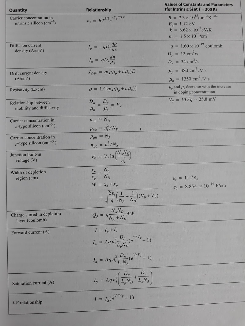
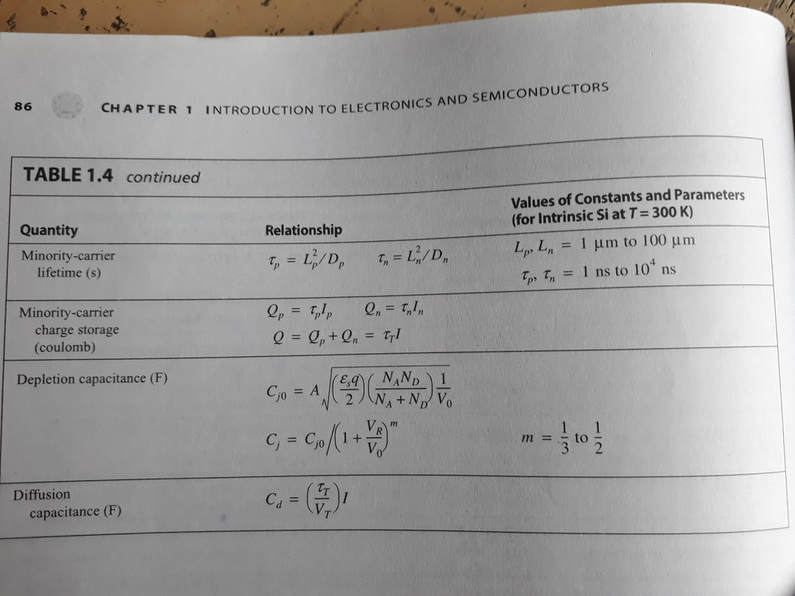
LIST OF IMPORTANT FORMULAE FOR MODULE 1.1
(taken from Microelectronics circuits - Sedra and Smith )
LIST OF IMPORTANT FORMULAE FOR MODULE 1.1
(taken from Microelectronics circuits - Sedra and Smith )
COMPLETION OF MODULE 1.1
COMPLETION OF MODULE 1.1
Lecture 08 handouts dated 21-07-2017
| edc_08.pdf |
Announcement :
1. Complete remaining 13 clipper circuits with Ideal diode and Constant voltage model in your note books by 24-07-2017.
2. Please note that Note books should be completed from start till date, because same will be checked during Lab sessions.
1. Complete remaining 13 clipper circuits with Ideal diode and Constant voltage model in your note books by 24-07-2017.
2. Please note that Note books should be completed from start till date, because same will be checked during Lab sessions.
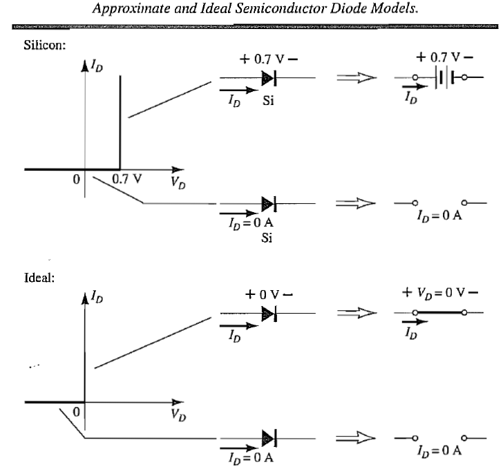
Refer Razavi electronic 1 , Lec 6 : For topic on diode models and observations
(start video from 6 minutes 30 sec and watch it till 35 minutes)
Refer Razavi electronic 1 , Lec 6 : For topic on Clipper circuits
(start video from 47 minutes 40 sec and watch it till 63 minutes 33 sec )
Refer Razavi electronic 1 , Lec 7 : For topic on Application of Diode
(start video from 11 minutes 25 sec and watch it till 25 minutes 33 sec )
Lecture 09 handout dated 24-07-2017
Refer Razavi electronic 1 , Lec 09 : For topic on Practical examples of Diode Circuits
(start video from 32 minutes 10 sec and watch it till 38 minutes 55 sec )
(start video from 32 minutes 10 sec and watch it till 38 minutes 55 sec )
Refer Razavi electronic 1 , Lec 12 : For topics on Limiters and Clampers
(start video from 7 minutes 20 sec and watch it till 14 minutes ) --- For Clippers / limiters
(start video from 23 minutes and watch it till 41 minutes 02 sec) --- For Clampers / Level shifters
(start video from 7 minutes 20 sec and watch it till 14 minutes ) --- For Clippers / limiters
(start video from 23 minutes and watch it till 41 minutes 02 sec) --- For Clampers / Level shifters
Lecture 10 handout dated 25-07-2017
Lecture 10 handout dated 25-07-2017
| edc_1_clamper_2017.pdf |
Announcement :
1. Please complete the following 6 Clamper circuits with constant voltage model in your books
2. Without resistor present in a clamper circuit is called an Ideal Clamper.
3. Practical clamper circuits have resistors connected as shown in image below With One Condition
(Condition: RC time constant should be large enough to ensure that voltage across capacitor does not discharge significantly during the period the diode if OFF. )
4. Add this condition as assumption in your clamper answers when asked in exam.
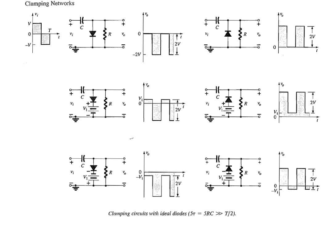
Above image taken from Boylestad book
Refer Week3 lec17 video below : For topics on Detailed Clamper circuits
(start video from 14 minutes 22 sec and watch it till end) --- For Clampers / Level shifters
Refer Week3 lec18 video below : For topics on Detailed Clamper circuits
(start video from start and watch it till 7 minutes 15 sec) --- For Clampers / Level shifters
(start video from start and watch it till 7 minutes 15 sec) --- For Clampers / Level shifters
COMPLETION OF MODULE 1.2
COMPLETION OF MODULE 1 : ( EDC lec 01 to EDC lec 10)
Topics covered so far :
PN junction Diode Analysis and applications. (08hours) ---- Completed in 10 lectures
1.1 PN junction Diode: Basic Structure, Energy Band Diagrams, Zero Applied Bias, Forward bias, Reverse bias, PN junction current, drift and diffusion current, junction capacitance, , DC load line, small signal model , Applied Bias, Reverse Applied Bias, temperature effects.
1.2 Clippers and Clampers
Lecture 11 handout dated 26-07-2017
Lecture 11 handout dated 26-07-2017
| edc_11.pdf |
| zener_breakdown_zener_ratings.pdf |
Note : For Zener construction topic can refer the above ebooks (Flyod)
Zener as Shunt regulator Numerical dated 14-08-2017
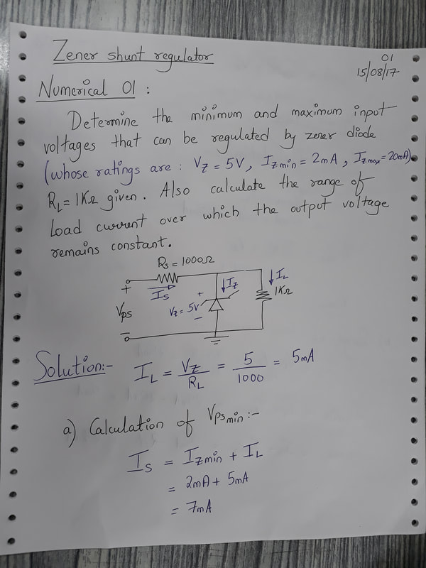
Zener as Shunt regulator Numerical shown in two videos below
Rectifier topic Started here :
Lecture 12 handout dated 28-07-2017
| edc_12.pdf |
| edc_power_supply_block.pdf |
| edc_power_supply_importance.pdf |
| edc_half_wave_rectifier_working.pdf |
Lecture 13 handout dated 31-07-2017
| edc_half_wave_rectifier_analysis.pdf |
Lecture 14 handout dated 01-08-2017
| edc_full_wave_center_tap_rectifier_working.pdf |
| edc_full_wave_center_tap_rectifier_analysis.pdf |
Announcement :
1. Please complete the Numerical 01 in your note books.
2. Please complete the topic of Ripple factor and its derivation in your note books.
1. Please complete the Numerical 01 in your note books.
2. Please complete the topic of Ripple factor and its derivation in your note books.
Lecture 15 handout dated 02-08-2017
| edc_full_wave_bridge_rectifier_analysis_and_working.pdf |
| edc_transformer_utilization_factor_for_rectifier_circuits.pdf |
Please Note :
1. In the lecture dated 02-08-2017, the TUF for center tap rectifier was calculated incorrectly, kindly correct it in ur notebooks from the above pdf.
2. If possible, complete the TUFs for half-wave, full wave center tap and full wave bridge rectifier in your notebooks from the above pdfs.
1. In the lecture dated 02-08-2017, the TUF for center tap rectifier was calculated incorrectly, kindly correct it in ur notebooks from the above pdf.
2. If possible, complete the TUFs for half-wave, full wave center tap and full wave bridge rectifier in your notebooks from the above pdfs.
Refer video below : For topics on TUF for Half wave and full wave bridge rectifier
(start video from start and watch it till the end)
(start video from start and watch it till the end)
Refer video below : For topics on TUF for full wave center tapped rectifier
(start video from start and watch it till the end)
(start video from start and watch it till the end)
COMPLETION OF MODULE 5.1
Lecture 16 handout dated 04-08-2017
| edc_filter_intro.pdf |
Lecture 17 handout dated 07-08-2017
Lecture 17 handout dated 07-08-2017
| edc_inductor_filter.pdf |
| edc_capacitor_filter.pdf |
Lecture 18 handout dated 08-08-2017
Lecture 18 handout dated 08-08-2017
| edc_lc_filter.pdf |
Lecture 19 handout dated 09-08-2017
Lecture 19 handout dated 09-08-2017
| edc_pi_filter.pdf |
| edc_filter_summary.pdf |

| edc_filter_numericals.pdf |
COMPLETION OF MODULE 5.2
Lecture 20 handout dated 11-08-2017
| edc_rectifier_filter_design_01.pdf |
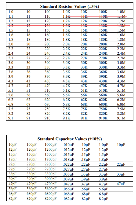
Standard Value of Resistor and capacitors : Helpful in design problems
Lecture 21 handout dated 14-08-2017
Lecture 21 handout dated 14-08-2017
| edc_rectifier_filter_design_02.pdf |
Rectifier and Filter topic ended here (lec 21)
JFET topic begins here (lec 22)
Lecture 22 handout dated 16-08-2017
Lecture 22 handout dated 16-08-2017
| edc_n_channel_jfet_01.pdf |
| edc_n_channel_jfet_02.pdf |
Can Refer below videos for JFET related concepts
Lecture 23 handout dated 18-08-2017
| edc_n_channel_jfet_03.pdf |
| edc_n_channel_jfet_04.pdf |
Completion of JFET topic (lec 23)

Lecture 24,25 and 26 handout dated 21-08-2017, 22-08-2017 and 23-08-2017
| edc_n_channel_enhancement_mosfet.pdf |
NOTE: 1. The MOSFET handout above is quite vast, as it contains detailed explanation. ( USE is wisely)
2. The derivation of drain current Id is not expected in exam.
2. The derivation of drain current Id is not expected in exam.
NOTE : In the video lectures 29 and 30, the derivation of Id is not expected in exam.
ANNOUNCEMENTS:
1. MID TERM break dates : 25th August to 29th August 2017 ( No lectures and labs during this period)
2. Quiz Test (Marks : 50M ) on 29th August 2017 (Only Multiple choice Questions and its open book test)
3. Assignment 1 and 2 will be uploaded soon ( Date of submission of both assignment will be 30th August 2017)
4. Experiment writeups to be completed in all aspects ( will be corrected during next lab session)
ANNOUNCEMENTS:
1. Submission date for EDC1 assignment 01 and 02 extended from 30th August to 1st September from 9:00 to 9:30 only
2. Kindly attach both the assignment's questions along with the assignment solution.
3. EDC 01 QUIZ TEST 01 updated marks are available in blackboard.
( In order to check question wise marks, login in to blackboard , select EDC course, then go to course tools , next click on my grades, next select EDC 01 Quiz 01 , next u will see ur marks in Blue in form of number, Click on the number , u will get your detailed marks questionwise. )
4. There were 4 questions, whose multiple - choice answers were given either incorrect or there was mistake in correct option, such 4 questions were already overridden in MARKS and FULL CREDIT were given to Answers of such questions.
EDC 1 Assignment 01
| edc1_assignment_01.pdf |
NOTE: In question number 16 of edc1 assignment 01 , assume the values of voltages V, V1 and V2 as 1 volt.
EDC 1 Assignment 02
| edc1_assignment_02.pdf |
Why attempting EDC Assignment 01 and 02 will be beneficial :
1. You can get Max 50 marks for each assignment, while will be scaled down and converted into marks in your TERM WORK.
2. Every university paper, 40-50 marks questions will be asked as per module per paper
3. Helpful in understanding some of the EDC1 practicals for which you have practical and oral examination.
4. These topics will have 100% marks coverage for MID TERM 1 ( that's 20 marks in MID TERM 01)
PIECE of Advice : DO IT YOURSELF
EDC1 QUIZ 1: ( Test will available on blackboard at 1pm sharp)
DATE : 29th August 2017
Time window : 1pm to 3pm
a) A student can give the test within the above time window, i.e one can start the test latest by 2pm
b) Test Results will be available by 3:30 pm on 29th August 2017 on blackboard
Description
Test consists of 50 questions of 1 marks each
Total time: 60 minutes
Total Marks: 50 M
Instructions
1. Choose the correct option from the four options available.
2. Read the questions carefully before answering
3. Keep calculator nearby
4. Keep a rough sheet nearby for scribbling
Timed Test
This test has a time limit of 1 hour.
Timer Setting
This test will save and submit automatically when the time expires.
Force Completion
Once started, this test must be completed in one sitting. Do not leave the test before clicking Save and Submit.
Lecture 27 handout dated 31-08-2017
| edc_n_channel_enhancement_mosfet_summary.pdf |
NOTE: Above summary pdf on NMOS -E type device is a concised version of earlier handout ( Can use in exam for writing the answer on NMOS-Enhancement type device)
Lecture 28 handout dated 01-09-2017
Lecture 28 handout dated 01-09-2017
| edc_p_channel_enhancement_mosfet.pdf |
Lecture 29 handout dated 04-09-2017
Lecture 29 handout dated 04-09-2017
| edc_n_channel_depletion_mosfet.pdf |
| edc_n_channel_depletion_mosfet_a.pdf |
| edc_p_channel_depletion_mosfet.pdf |
Holiday on 05-09-2017
SE Defaulter's and attendance record available on blackboard
Lecture 30 dated 06-09-2017 : Revision Lecture
Lecture 30 dated 06-09-2017 : Revision Lecture
EDC 1 Syllabus for MIDTERM 01 updated on 06 - 09-2017
Module 01: PN junction Diode Analysis and applications
1.1 PN junction Diode: Basic Structure, Energy Band Diagrams, Zero Applied Bias, Forward bias, Reverse bias, PN junction current, drift and diffusion current, junction capacitance, DC load line, small signal model, Applied Bias, Reverse Applied Bias, temperature effects.
(Derivations + Numericals inclusive)
1.2 Clippers and Clampers
Module 03: Field Effect Devices
3.1 JFET: Construction, operation, and characteristics. (Numericals inclusive )
MOSFET: Construction, operation, and characteristics of D-MOSFET and E-MOSFET.
Module 04: Special semiconductor devices – I
4.1 Construction, working, and characteristics of Zener diode
Module 05: Rectifiers and Regulators
5.1 Rectifiers: working and analysis of Half wave, Full wave and Bridge (Derivations + Numericals inclusive)
5.2 Filters: C,L,LC, pi (No Derivations on ripple factor for filter topic in Mid term 01)
5.3 Regulators: Zener shunt regulator (Numericals inclusive )
Module 06 : Design of electronic circuits
6.3 Design of full wave rectifier with LC and pi filter
EDC 1 MIDTERM 01 QUESTION PAPER
| edc1_mid_term_1_2017.pdf |
EDC 1 MIDTERM 01 SOLUTION : updated on 9th September, 2017
| edc_1_mid_term_1_solution_2017.pdf |
EDC 1 MIDTERM 02 topics starts from here on:
Lecture 31 supporting material dated 11-09-2017 : coming soon
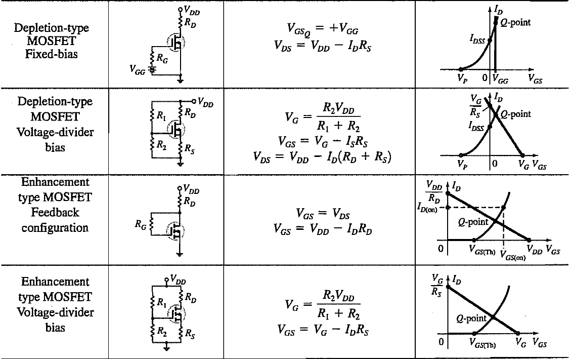
Topics Covered : Depletion type MOSFET dc biasing: 1. Fixed bias dc biasing, 2. Zero bias dc biasing and 4. Self bias dc biasing and Derivation of Q point derivation for above biasing circuits. Location of Q point on DC load line for above Biasing circuits
Lecture 32 supporting material dated 12-09-2017 : coming soon
Topics Covered : Depletion type MOSFET dc biasing: 1. Voltage Divider dc biasing and Derivation of Q point derivation for above biasing circuits. Location of Q point on DC load line for above Biasing circuits. Numericals on Zero Biasing, Self biasing and Voltage divider Biasing using NMOS-D type MOSFET.
ANNOUNCEMENTS:
1. Students can check their individual Mid term 1 papers on 14-09-2017
2. Timings : 9 to 9:30 am,12:30 to 1 pm
3. Come in a group of 5 together for smooth processing
Lecture 33 supporting material dated 13-09-2017 : coming soon
Topics Covered : Enhancement type MOSFET dc biasing: 1. Drain feedback biasing and Voltage Divider dc biasing and Derivation of Q point derivation for above biasing circuits. Location of Q point on DC load line for above Biasing circuits. Numericals on Voltage divider Biasing using NMOS-E type MOSFET.
Refer Boylestad indian edition ebook
Topic : D Type MOSFET biasing : Pg 420-423
Topic : E type MOSFET biasing : Pg 425-430
Lecture 34 supporting material dated 15-09-2017 :
Topics Covered : Numericals on Voltage divider Biasing using NMOS-E type MOSFET and Drain feedback biasing , PMOS -E type voltage divider biasing , Effect of connection VSS on biasing circuits, Design steps for NMOS-E type Voltage divider biasing and self biasing
| edc1_design01_nmos_e_type_vdb.pdf |
NOTE: During the lecture dated 15-09-2017, Design 01 discussed in class was not correct. Please find the correct version of design 01 in above pdf.
|
THIS IS NOT CORRECT
| ||
NOTE : Please write the design steps for biasing circuits in your notebooks
CORRECTION : NOTE IN DESIGN STEPS FOR E TYPE MOSFET , SELF BIASING i.e for VGS negative is not POSSIBLE
In the above pdf it is given for self biasing, please note that is wrong, In case of Enhancement type biasing VGS can only take postive values, i.e only Design that is possible for E type MOSFET is
i) Drain feedback biasing and 2) Voltage divider biasing
In the above pdf it is given for self biasing, please note that is wrong, In case of Enhancement type biasing VGS can only take postive values, i.e only Design that is possible for E type MOSFET is
i) Drain feedback biasing and 2) Voltage divider biasing
|
THIS IS CORRECT
| ||
PLEASE REFER the above correction version of E type MOSFET Designing steps
ANNOUNCEMENTS: (updated on 15-09-2017)
1. Students scoring less than 8 marks only in EDC 1 Mid term 01 are required to solve MID term paper again in separate both sides ruled sheets and submit the same by 18-09-2017
2. Give the heading of above work as Action assignment 01
3. Entire Class do solve the HOME WORK 01 numericals updated below, same will be checked on 18-09-2017
HOME WORK 01 NUMERICALS :
| edc1_homework01.pdf |
Lecture 35 supporting material dated 18-09-2017 :
Topics Covered : Design steps for NMOS-D type Voltage divider biasing and self biasing, Introduction to MOSFET Amplifier topic, Importances of location of Q point on DC load line, Concept of SMALL SIGNAL MODEL and its parameters.
Topics Covered : Design steps for NMOS-D type Voltage divider biasing and self biasing, Introduction to MOSFET Amplifier topic, Importances of location of Q point on DC load line, Concept of SMALL SIGNAL MODEL and its parameters.
| design_of_depletion_type_n_channel_mosfet_biasing_circuit.pdf |
| edc1_nmos_small_signal_model.pdf |
COMPLETION OF MODULE 3.2
MOSFET AMPLIFIER BEGINS FROM HERE
Lecture 36 supporting material dated 19-09-2017 :
Topics Covered : NMOS-E common source amplifier analysis, derivation of voltage gain Av for NMOS-E amplifier
Topics Covered : NMOS-E common source amplifier analysis, derivation of voltage gain Av for NMOS-E amplifier
Refer Razavi electronic 1 , Lec 32 : For topic on MOSFET amplifier and concept of transconductance
NOTE: While watching, only concentrate on understanding the concepts
(start video from 17 minutes 34 sec and watch it till the end )
NOTE: While watching, only concentrate on understanding the concepts
(start video from 17 minutes 34 sec and watch it till the end )
Refer Razavi electronic 1 , Lec 33 : For topic on concept of Small signal Model
NOTE : The large signal model explained in this video lecture is NOT in EDC1 syllabus
(start video from 21 minutes 34 sec and watch it till the end )
NOTE : The large signal model explained in this video lecture is NOT in EDC1 syllabus
(start video from 21 minutes 34 sec and watch it till the end )
Refer Razavi electronic 1 , Lec 34: For topic on concept of Small signal Model of PMOS device and inclusion of ro in small signal model
NOTE : The derivations explained in this video lecture is NOT in EDC1 syllabus, only concentrate on understanding the concepts
(start video from beginning and watch it till the end )
NOTE : The derivations explained in this video lecture is NOT in EDC1 syllabus, only concentrate on understanding the concepts
(start video from beginning and watch it till the end )
Refer Razavi electronic 1 , Lec 35: For topic on properties of MOSFET amplifier, concept of Common source amplifier, derivation of Av for NMOS amplifer
NOTE: While watching, only concentrate on understanding the concepts
(start video from 38 minutes 06 sec and watch it till the end )
For applications topics on MOSFET : (start video from 10 minutes 22 sec and watch it till 34 minutes and 15 sec )
NOTE: While watching, only concentrate on understanding the concepts
(start video from 38 minutes 06 sec and watch it till the end )
For applications topics on MOSFET : (start video from 10 minutes 22 sec and watch it till 34 minutes and 15 sec )
Lecture 37 supporting material dated 22-09-2017 :
Topics Covered : NMOS-E common source amplifier analysis, derivation of input and output impedance for NMOS-E amplifier, Problem of gain variation in CS stage, NMOS-E common source degenaration stage and derivation of gain for the same.
Refer Razavi electronic 1 , Lec 36: For topic on Input and output impedane in amplifers
NOTE: While watching, only concentrate on understanding the concepts
(start video from 55 minutes 51 sec and watch it till the end )
Refer Razavi electronic 1 , Lec 37: For topic on problem of gain variation in CS stage
NOTE: While watching, only concentrate on understanding the concepts
(start video from 57 minutes 48 sec and watch it till the end )
Refer Razavi electronic 1 , Lec 37: For topic on problem of gain variation in CS stage
NOTE: While watching, only concentrate on understanding the concepts
(start video from 57 minutes 48 sec and watch it till the end )
Refer Razavi electronic 1 , Lec 38: For topic on degenarated CS stage
NOTE: While watching, only concentrate on understanding the concepts
(start video from 05 minutes 22 sec and watch it till 22 minutes 12 sec )
NOTE: While watching, only concentrate on understanding the concepts
(start video from 05 minutes 22 sec and watch it till 22 minutes 12 sec )
Lecture 38 supporting material dated 23-09-2017 :
Topics Covered : NMOS-E common source degenaration stage and derivation of Rin and Rout for the same, numerical on CS amplifer , NMOS-E common gate configuration and derivation of gain for the same
Refer Razavi electronic 1 , Lec 39:
NOTE: While watching, only concentrate on understanding the concepts
(start video from 04 minutes 22 sec and watch it till 11 minutes 18 sec ) : only for input and out impedance of Degenerated CS stage
(start video from 11 minutes 18 sec and watch it till 53 minutes 55 sec ) : only for concept of biasing a CS stage and concept of attenutation at input side, concept of loop antenna , reduced senstivity with degenerated CS stage, concept of (Drain feedback or SELF bias CS stage) (only for interested readers)
(start video from 59 minutes 18 sec and watch it till 11 minutes 18 sec ) : only for common gate topology concept
Lecture 39 dated 25-09-2017 : Cancelled due to absence of teacher
Lecture 39 supporting material dated 26-09-2017 :
Topics Covered : NMOS-E common gate configuration and derivation of voltage gain for the same (revision) , derivation input and output impedance of CG amplifer . NMOS-E common Drain (SOURCE FOLLOWER) configuration and derivation of voltage gain, input impedance and output impedance for the same, Summary of CS stage, CS stage with degeneration, CD stage and CG amplifier stage, NUMERICAL 02 ( based on depletion type CS amplfier)
Refer Razavi electronic 1 , Lec 40:
NOTE: While watching, only concentrate on understanding the concepts
(start video from 03 minutes 33 sec and watch it till 18 minutes 45 sec ) : only for derivation of voltage gain , input impedance and output impedance of CG stage, Application of CG stage is also inclusive in this video
Refer Razavi electronic 1 , Lec 41:
NOTE: While watching, only concentrate on understanding the concepts
(start video from 04 minutes 39 sec and watch it till 38 minutes 58 sec ) : only for derivation for voltage gain and input impedance for Source follower , application of Source follower circuit
(start video from 56 minutes 44 sec and watch it till the end ) : only for summary on CS stage , CS stage with degeneration, CD stage and Source follower stage)
Lecture 40 supporting material dated 27-09-2017 :
Topics Covered : Derivation of voltage gain , input impedance and output impedance for E type NMOS drain feedback amplfier, Numerical 03 (based on E type NMOS drain feedback amplfier) Self bias MOSFET amplifier analysis , Numerical 04 ( based on CS amplifer without capacitor Cs and having dual power supply) , Numerical 05 ( based on CG amplifier using D type NMOS ) , Numerical 06 ( based on CD amplifier using D type NMOS)
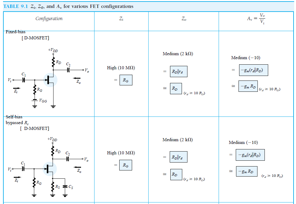
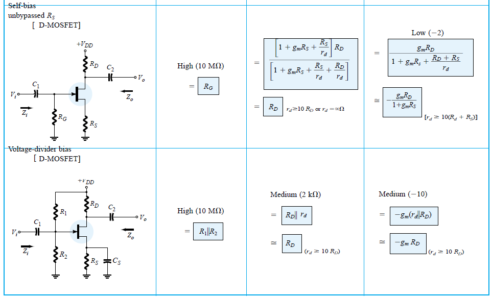
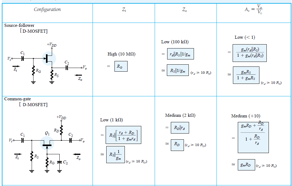
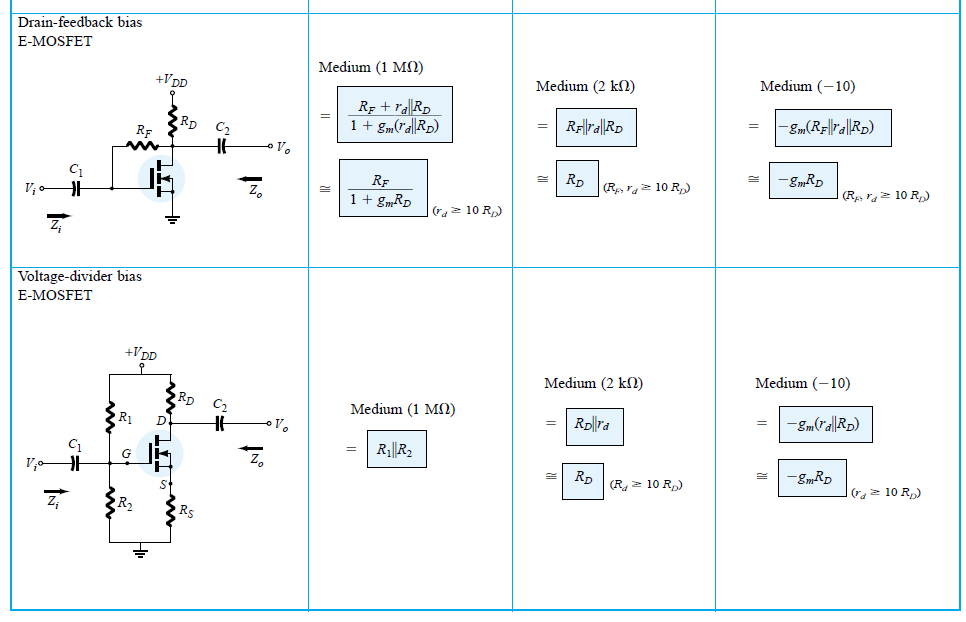
NOTE: In TABLE 9.1 : Wherever you see rd >= 10 RD, it means rd value is considered high and hence kept open compared to RD or RS resistor
ANNOUNCEMENTS: (updated on 27-09-2017)
1. Entire Class do solve numerical 05 and 06 given during lecture 40, same will be checked on 29-09-2017
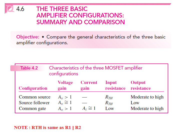
2. Please complete the table 4.2, given in image below in your note books
COMPLETION OF MODULE 3.3
Lecture 41 dated 29-09-2017 : Cancelled due to absence of teacher
Lecture 41 supporting material dated 03-10-2017 :
Topics Covered : Bipolar junction transistor device structure and working of npn bjt in Active mode
Lecture 42 supporting material dated 04-10-2017 :
Topics Covered : Details of terminal currents in an npn bjt: the base current, the emitter current and the collector current. Relation between alpha and beta, condition for npn bjt to remain in active mode of operation.
| edc1_bjt_fundamentals_voltage_current_relations.pdf |

Lecture 43 supporting material dated 06-10-2017 :
Topics Covered : Summary of current-voltage relationships for npn bjt to be in active region, Common- emitter configuration : Input and output characteristics, Common-base characteristics and common collector characteristics.
NOTE: For Common- emitter configuration : Input and output characteristics, Common-base characteristics and common collector characteristics topic : Refer Ebook Robert Boylestad, Electronic Devices and circuit theory
Lecture 44 supporting material dated 06-10-2017 : coming soon
Topics Covered : BJT DC biasing: Fixed bias without and with RE analysis i.e derivation of Q point and equation of DC load line. voltage divider bias analysis i.e derivation of Q point and equation of DC load line
Topics Covered : BJT DC biasing: Fixed bias without and with RE analysis i.e derivation of Q point and equation of DC load line. voltage divider bias analysis i.e derivation of Q point and equation of DC load line
Refer Ebook Robert Boylestad, Indian scanned edition , Electronic Devices and circuit theory for Lecture 44
Pages 161 - 176, exclude the data which is not covered in class during lecture 44
Pages 161 - 176, exclude the data which is not covered in class during lecture 44
EDC 1 Assignment 03 : uploaded on 10-10-2017 by 2:30 pm
| edc1_assignment_03.pdf |
DATE OF SUBMISSION for EDC 1 Assignment 03 : 14-10-2017
ANNOUNCEMENT related to EDC 1 MIDTERM 2, mini project and QUIZ 2 :(updated on 11-10-2017)
1. Refer to class work notes for midterm 2
2. Focus on the topics covered in classroom during lecture 31 to 44
3. B3 and B4 will wait after their EDC 1 for confirmation of their mini project topics.
4. B2 and B1 will finalize the self-chosen topics latest by 11-10-2017
5. Quiz 2 will be active on blackboard on 11-10-2017 from 1:30 to 4:30 pm
EDC1 QUIZ 2: ( Test will available on Blackboard at 1: 30 pm instead of 12:30 pm sharp)
DATE: 11th October 2017
Time window : 1:30pm to 4:30pm
a) A student can give the test within the above time window, i.e one can start the test latest by 2:50 pm
b) Test Results will be available by 6:00 pm on 11th October 2017 on blackboard
Description
Test consists of 50 questions of 1 marks each
Total time: 100 minutes
Total Marks: 50 M
Instructions
1. Choose the correct option from the four options available.
2. Read the questions carefully before answering
3. Keep calculator nearby
4. Keep a rough sheet nearby for scribbling
Timed Test
This test has a time limit of 100 minutes
Timer Setting
This test will save and submit automatically when the time expires.
Force Completion
Once started, this test must be completed in one sitting. Do not leave the test before clicking Save and Submit.
EDC 1 Syllabus for MIDTERM 02 updated on 06-10-2017
Module 02 : Bipolar Junction Transistor ( 05 marks )
2.1 BJT operations, voltages and currents, BJT characteristics ( CE, CB, CC configurations) , early effect (Not in Mid term 02 syllabus)
2.2 DC Circuit Analysis: DC load line and region of Operation, Common Bipolar Transistor Configurations, biasing circuits, analysis (Derivation + Numericals - only Fixed bias and voltage divider bias )
Module 03 : Field Effect Devices (05 + 10 Marks)
3.2 DC Circuit Analysis : DC load line and region of operation, Common-MOSFETs configurations, Analysis and Design of Biasing Circuits
3.3 AC Analysis: AC load line (Not in Mid term 02 syllabus) , Small-Signal model of MOSFET and its equivalent Circuit, Small-Signal Analysis MOSFET Amplifiers ( Common-Source, Source Follower, Common Gate)
MINI PROJECT updated on 03 -10 -2017
List of closed topics : ( For B1,B2,B3 and B4 batches)
1. Headphone amplifier
2. Transistor tester
3. DC power supply ( 230 V to 5 V dc)
4. DC power supply (230 V to -5V dc , 0 and 5V dc)
5. USB mobile charger circuit
NOTE:
1. Open ended topics ( Students choice topics) : Should be finalized on or before 11-10-2017 batchwise
2. The groups for mini- projects shall be strickly as per maintained during Lab sessions.
3. Verification on breadboard deadline : 14-10-2017
MINI PROJECT final list updated batch-wise on 19 -10 -2017
B1 batch:
Groups (Sap IDs)
G11(01,02,03): DC power supply (230 V to -5V dc , 0 and 5V dc)
G12(04,05,06): DC power supply ( 230 V to 5 V dc)
G13(07,08,09): Fire alarm
G14(10,11,12): USB charger
G15(13,14,15): Headphone amplifier
G16(16,17,18): Lazer Trip circuit
G17(19,20): Water-level Indicator
B2 batch:
Groups (Sap IDs)
G21(21,22,23): DC power supply ( 230 V to 5 V dc)
G22(24,25,26): Transistor tester
G23(27,28,29): DC power supply (230 V to -5V dc , 0 and 5V dc)
G24(30,31,32): USB charger
G25(33,34,35): Headphone amplifier (changed) to BJT series regulator
G26(36,37,38,39): Temperature detector
B3 batch:
Groups (Sap IDs)
G31(40,41,42): Headphone amplifier (changed) to Touch Sensor
G32(43,44,45): USB charger
G33(46,47,48): DC power supply (230 V to -5V dc , 0 and 5V dc)
G34(49,50,51): DC power supply ( 230 V to 5 V dc)
G35(52,53,54): Astable Multivibrator
G36(55,56): Light Detector
G37(57,58): Music Controlled Lightning
B4 batch:
Groups (Sap IDs)
G41(59,60,61): Transistor tester
G42(62,63,50009): Headphone amplifier (changed) to Water Level Indicator
G43(8001,8002,8003): Light detector
G44(8004,8005,8006): DC power supply (230 V to -5V dc , 0 and 5V dc)
G45(8007,8008,8009): USB charger
G46(8010,8011,8012): DC power supply ( 230 V to 5 V dc)
The above list is final, if there are any mistakes in the names of the mini-projects, inform latest by 12-10-2017
EDC 1 MIDTERM 02 QUESTION PAPER
| edc1_mid_term_2_2017.pdf |
EDC 1 MIDTERM 02 SOLUTION : updated on 12th October, 2017
| edc_1_mid_term_2_solution_2017.pdf |
MINI PROJECT ANNOUNCEMENTs updated on 13 -10 -2017
NOTE:
1. Verification on breadboard deadline : 14-10-2017 (Only for B2 batch)
2. Verification on breadboard deadline : 15-10-2017 (Only for B1 batch)
3. Verification on breadboard deadline : 16-10-2017 (Only for B3 batch)
4. Verification on breadboard deadline : 16-10-2017 (Only for B4 batch)
5. Those groups who have completed their breadboard verification can report before the above dates too
Lecture 45 supporting material dated 13-10-2017 : coming soon
Topics Covered : BJT DC biasing: Early effect concept and its effect on Common Emitter Output characteristics, Collector to base bias without and with RE analysis i.e derivation of Q point
Lecture 46 supporting material dated 14-10-2017 : coming soon
Topics Covered : BJT DC biasing: Necessity for DC biasing, Numerical 01 on fixed bias,Numerical 02 on emitter bias, How stability improves in emitter bias, Numerical 03 on Collector to base bias with and without RE, How stability is achieved in Collector to base bias without and with RE
Lecture 47 supporting material dated 15-10-2017 : coming soon
Topics Covered : BJT DC biasing: Revision on Derivation of Q point expression for Voltage divider bias using npn BJT, How stability is achived in VDB, Numerical 06 : Determination of Q point for Voltage divider bias, Plotting of DC load line and determining the region of operation, Need of Stabilization of Q point
Lecture 48 supporting material dated 15-10-2017 : coming soon
Topics Covered : Derivation for general expression for Stability factor, Derivation for stability factor for 1) Fixed bias 2) Emitter bias 3) Collector to base bias 4) Collector to base bias with RE 5) Voltage divider bias, Design Steps for Fixed bias and Emitter bias, Design numericals Design 01 and Design 02
Topics Covered : Derivation for general expression for Stability factor, Derivation for stability factor for 1) Fixed bias 2) Emitter bias 3) Collector to base bias 4) Collector to base bias with RE 5) Voltage divider bias, Design Steps for Fixed bias and Emitter bias, Design numericals Design 01 and Design 02
Lecture 49 supporting material dated 16-10-2017 :
Topics Covered : Voltage divider bias circuit for PNP transistor, Common base configuration DC analysis and numerical , Numerical 07 based on two power supplies for Voltage divider bias circuit, Design 03 to design voltage divider bias circuit using NPN transistor
Lecture 50 supporting material dated 17-10-2017 :
Topics Covered : Bias stability and bias compensation: Diode compensation for Ico, Diode Compensation for VBE, Bias Compensation using thermistor
Topics Covered : Bias stability and bias compensation: Diode compensation for Ico, Diode Compensation for VBE, Bias Compensation using thermistor
COMPLETION OF MODULE 2.2
COMPLETION OF 70% EDC 01 syllabus from 10-07-2017 (EDC lecture 01) to 17-10-2017 (EDC lecture 50)
ANNOUNCEMENT related to EDC 01 Assignment 04, TERM END Submission and Mini-projects :(updated on 19-10-2017)
1. Diwali vacation period from 18-10-2017 to 22-10-2017
2. In the light of completion of EDC 01 assignments 01,02 and 03 on time, there is no assignment 04
3. Happy Diwali to one and all.
4. EDC 01 journal shall consist of Total 12 experiments + 3 Assignments + 1 mini project report
5. The date for Term Work journal Submission .... coming soon....
6. Dates for performing hardware experiments (for practice or for those who have missed their practicals ): 23-10-2017, 24-10-2017 and 25-10-2017
7. EDC 01 Practical Examination dates: 6-11-2017 and 07-11-2017
8. Dates for mini project presentation and demonstration on general purpose PCB :
a) Mini project presentation : Not more than 3 minutes per group
b) B1 & B2 batch : 26-10-2017 from 11 to 12 pm
c) B3 & B4 batch : 26-10-2017 from 12 to 1 pm
9. EDC 01 extra lectures on 23-10-2017, 24-10-2017, 25-10-2017 and 26-10-2017 from 7:30 to 9 am
Topic: BJT amplifier analysis and design of single stage CE amplifier
10. Dates for EDC 01 Experiments checking: 23-10-2017, 24-10-2017, 25-10-2017(till 12 pm) , 26-10-2017, and 27-10-2017
ANNOUNCEMENT related to Mid term Test 1 for defaulters :(updated on 20-10-2017)
1. Test will conducted on 25-10-2017 from 7 to 8 am
1. Test will conducted on 25-10-2017 from 7 to 8 am
MINI PROJECT REPORT FORMAT .... updated on 25-10-2017
Dates for mini project presentation and demonstration on general purpose PCB :
a) Mini project presentation : Not more than 3 minutes per group
b) B1 & B2 batch : 26-10-2017 from 11 to 12 pm
c) B3 & B4 batch : 26-10-2017 from 12 to 1 pm
1. For 26-10-2017, carry a copy of your mini project report.
2. Follow the 3 minute presentation time strictly
3. In project title file, please change MINOR PROJECT REPORT to MINI PROJECT REPORT
| edc1_mini_project.pdf |
| project_title_page_format.docx |
EDC 1 experiment checking timings .... updated
on 27-10-2017
Batch-wise timings :
A) 27-10-2017
B1 batch : 8 to 9am & 1 to 2 pm
B2 batch : 9 to 10 am & 2 to 3 pm
B4 batch : 10 to 11 am & 3 to 4 pm
B3 batch : 12 to 1 pm & 4 to 5 pm
A) 28-10-2017
B3 batch : 8 to 9am & 1 to 2 pm
B4 batch : 9 to 10 am & 2 to 3 pm
B2 batch : 10 to 11 am & 3 to 4 pm
B1 batch : 12 to 1 pm & 4 to 5 pm
EDC 1 experiment checking timings .... updated
on 31-10-2017
Day :1-11-2017
ALL batches: 11 am to 6 pm
First come First serve basis
NOTE:
1) All Group members of mini-project, kindly email the report latest by 1-11-2017 on [email protected] or [email protected]
2) Name Document as your Group Number example as G11
3) FINAL Submission Tentative DATE: coming soon
4) Assignment 1, 2 and 3 and midterm 2 EDC 1 papers will be available on Submission date only
EDC 1 Final Submission timings .... updated on 02-11-2017
Day :04-11-2017
Journal Submission TIMINGS: 2 to 4 pm (ALL BATCHES)
PRACTICAL EXPERIMENTS ORIENTATION TIME: 12 to 2 pm
Remaining experiments checking time: 4 to 6 pm
NOTE:
1) EDC 1 JOURNAL shall consist of
a) MINI PROJECT REPORT duly signed and graded
b) Assignment 1, 2 and 3 duly checked and graded
c) 12 Experiments duly checked and graded and complete in all aspects
2) MAny students had not written post lab question for expt no. 12 and got their experiments checked, PLEASE NOTE Final Journal Submission will be STOPPED for such Students if questions not answered for Expt 12.
Electronic Devices and Circuits I Laboratory Batch wise dates updated by 25-10-2017
1) Students who have missed their practicals needs to complete them latest by 25-10-2017
2) While checking the experiments, if one has not performed the experiment, that experiment will not be checked.
3) Enter these practicals dates in your write-ups as per one's batch
EDC 1 Extra lectures to be scheduled between 13-11-2017 to 15-11-2017 from 8:30 am to 11:30 am
EXTRA EDC 1 Lecture 01 dated 13-11-2017 from 8:30 to 11:30
topics covered: AC analysis of BJT circuits, introduction to h parameter model and re model
topics covered: AC analysis of BJT circuits, introduction to h parameter model and re model
EXTRA EDC 1 Lecture 02 dated 14-11-2017 from 8:45 to 11:45
topics covered: AC analysis of BJT amplifiers circuits using h parameter model for CE and CB configurations + Numericals
topics covered: AC analysis of BJT amplifiers circuits using h parameter model for CE and CB configurations + Numericals
EXTRA EDC 1 Lecture 03 dated 15-11-2017 from 8:45 to 1:00 pm
topics covered: AC analysis of BJT amplifiers circuits using h parameter model for CC configurations + Numericals , Design Steps for Single stage CE amplifier + 1 design numercials for CE amplifier using voltage divider bias
topics covered: AC analysis of BJT amplifiers circuits using h parameter model for CC configurations + Numericals , Design Steps for Single stage CE amplifier + 1 design numercials for CE amplifier using voltage divider bias
COMPLETION OF MODULE 2.3
COMPLETION OF 85% EDC 01 syllabus from 10-07-2017 (EDC lecture 01) to 15-11-17 (EDC lecture 50+3 hours three lectures= Total 60 EDC lectures)
Following topics which we not covered for EDC -1 are:
FROM module 2.3: AC load line concept
FROM module 4.1: Construction, working and characteristics of Schottky diode, Varactor diode, Tunnel diode, Solar Cells, Photodiodes, LEDs
FROM module 5.3: Series and shunt regulator using single transistor and Zener
FROM module 6.2: Design of single stage CS MOSFET amplifier
Announcements updated on 23-11-2017
Handouts related to BJT DC biasing and AC analysis...... coming soon by 24-11-2017 or 25-11-2017
BJT DC biasing handout updated on 24-11-2017
Topics covered in handout : BJT construction, working, bjt configurations, bjt characteristics, analysis of transistor amplifier, Necessity of DC biasing, Need for stabilization, Analyses and numerical on various BJT biasing circuits(Fixed bias, Fixed emitter bias, Collector to base bias, Collector to base bias with RE, voltage divider bias), derivation of stability factor all biasing circuits, Bias compensation techniques
| edc1_bjt_dc_anaylsis.pdf |
BJT AC analysis handout updated on 24-11-2017
Topics covered in handout : BJT AC analysis : re model of bjt, h parameter model of bjt, Analysis of CE, CE without bypass capacitor, CC and CB amplifier using h parameter model with numerical. Comparison of CC, CE and CB amplifiers. Design steps for single stage CE amplifier, Design numerical on CE amplifier
| edc1_bjt_ac_anaylsis.pdf |
Type of Exam questions and miscellaneous topics like series regulator using bjt and zener, ac load line concept ,etc .... was not uploaded here, but handout images were send to a student
Electronic Devices and Circuits I Laboratory
Please note, completion of experiment in the lab, should be followed by written write-up for the same in the next practical turn.
| instructions_to_write_edc_1__journal.pdf |
Note: 1. Draw circuit diagrams as per given in lab session and not as given in write-up
2. Answer Post-Lab questions after the conclusion of the experiment.
2. Answer Post-Lab questions after the conclusion of the experiment.
Laboratory Experiment Rubrics
| laboratory_experiment_rubrics.pdf |
EXPERIMENT NO. 01 : DIODE I-V CHARACTERISTICS
| edc1_expt_01.pdf |
EXPERIMENT NO. 02 : CLIPPER AND CLAMPER CIRCUITS
| edc1_expt_02.pdf |
Note :
Expt 02 uploaded here is just a sample write up. The following changes every group has to follow:
1. Aim , Apparatus and Theory should be written as it is given in the write up.
2. In the writeup one sample clipper and clamper circuit is drawn, please draw 4 Clipper and 2 clamper circuits as per you'll have performed in a group.
3. Calclulations have to written on blank side for every clipper and clamper circuit. (USE Constant voltage model)
4. WAVEforms for 4 clippers and 2 clampers circuits should be drawn on Graph paper only.
5. If any doubts still, contact on [email protected]
EXPERIMENT NO. 03 : ZENER I-V CHARACTERISTICS
| edc1_expt_03.pdf |
EXPERIMENT NO. 04 : FULL WAVE CENTER TAP RECTIFIER WITH C FILTER
Updated on 24-10-2017
Updated on 24-10-2017
| edc1_expt_04.pdf |
EXPERIMENT NO. 05 : N-CHANNEL JFET OUTPUT AND TRANSFER CHARACTERISTICS
| edc1_expt_05.pdf |
EXPERIMENT NO. 06 : SPICE SIMULATION OF PN AND ZENER I-V CHARACTERISTICS
| edc1_expt_06.docx |
EXPERIMENT NO. 07: SPICE SIMULATION OF N-channel JFET OUTPUT AND TRANSFER CHARACTERISTICS
| edc1_expt_07.docx |
EXPERIMENT NO. 08: SPICE SIMULATION OF N-channel MOSFET OUTPUT AND TRANSFER CHARACTERISTICS
| edc1_expt_08.docx |
Instructions for Expt 06 to Expt 08
1. Download the latest version of open-source software LTspice from
http://www.linear.com/designtools/software/
2. For experiments 06, 07 and 08, only printouts of write-ups are required.
3. Sample write-up is given below, modify it and add your circuits, spice code, and all the simulation plots accordingly.
4. Anything in red in the write-up is just for your reference, please delete the red content from the write-up.
5. A word document file is uploaded, so you'll edit the contents accordingly.
6. Don't alter the theory in the Docx file.
7. Only simulation result calculations and conclusion in this experiment has to be handwritten.
8. The Batch representatives ( 2 per batch as per meeting on 24/08/2017) please take care of experiments 06 to 08. Before taking printout of experiments, forward it to email id: [email protected] for verification on or before 29th August 2017
ATTENTION entire SE class: PLEASE perform the simulation in LTspice once, before you submit your write-ups.
Verify the schematic, spice code and characteristics of devices. (DO IT YOURSELF) !!!!
EXPERIMENT NO. 09: N-channel MOSFET OUTPUT AND TRANSFER CHARACTERISTICS
Updated on 23-10-2017
| edc1_expt_09.pdf |
EXPERIMENT NO. 10: NMOS-E type Common Source amplifier and measurement of its performance parameters i.e Q Point , Voltage gain, input resistance and Output resistance
Updated on 24-10-2017
Updated on 24-10-2017
| edc1_expt_10.pdf |
EXPERIMENT NO. 11: NPN BJT COMMON EMITTER INPUT AND OUTPUT CHARACTERISTICS
Updated on 20-10-2017
Updated on 20-10-2017
| edc1_expt_11.pdf |
NOTE: Don't write anything given in RED in write up of EDC-1 experiment 11
EXPERIMENT NO. 12: SIMULATION STUDY OF DIFFERENT BIASING CIRCUITS USING NPN BJT.
Updated on 24-10-2017
NOTE: Follow instructions marked as RED in the write-up of experiment 12
| edc1_expt_12.pdf |
