"An investment in knowledge pays the best interest"
Course Objectives:
1. To teach fundamental principles of fabrication of VLSI devices and circuits
2. To disseminate knowledge about novel VLSI devices
1. To teach fundamental principles of fabrication of VLSI devices and circuits
2. To disseminate knowledge about novel VLSI devices
Course Outcome :
After successful completion of the course student will be able to
1. demonstrate a clear understanding of CMOS fabrication flow and technology scaling
2. demonstrate a clear understanding of various MOS fabrication processes, semiconductor measurements, packaging, testing and advanced semiconductor technologies
3. discuss physical mechanism in novel devices
4. verify processes and device characteristics via simulations
IC Technology Course Syllabus
Module 01 : Environment and Crystal Growth for VLSI Technology
Environment: Semiconductor technology trend, Clean rooms, Wafer cleaning
Semiconductor Substrate: Phase diagram and solid solubility, Crystal structure, Crystal defects, Czochralski growth, Bridgman growth of GaAs, Float Zone growth, Wafer Preparation and specifications
Module 02 : Fabrication Processes Part 1
Deposition: Evaporation, Sputtering and Chemical Vapor Deposition
Epitaxy: Molecular Beam Epitaxy, Vapor Phase Epitaxy, Liquid Phase Epitaxy, Evaluation of epitaxial layers
Silicon Oxidation: Thermal oxidation process, Kinetics of growth, Properties of Silicon Dioxide, Oxide Quality, high κ and low κ dielectrics
Diffusion: Nature of diffusion, Diffusion in a concentration gradient, diffusion equation, impurity behavior, diffusion systems, problems in diffusion, evaluation of diffused layers
Ion Implantation: Penetration range, ion implantation systems, process considerations, implantation damage and annealing
Module 03 : Fabrication Processes Part 2
Etching: Wet chemical etching, dry physical etching, dry chemical etching, reactive ion etching, ion beam techniques
Lithography: Photoreactive materials, Pattern generation and mask making, pattern transfer, Electron beam, Ion beam and X-ray lithography
Device Isolation, Contacts and Metallization: Junction and oxide isolation, LOCOS, trench isolation, Schottky contacts, Ohmic contacts, Metallization and Packaging
CMOS Process Flow: N well, P-well and Twin tub
Design rules, Layout of MOS based circuits (gates and combinational logic), Buried and Butting Contact
Module 04 : Measurements, Packaging and Testing
Semiconductor Measurements: Conductivity type, Resistivity, Hall Effect Measurements, Drift Mobility, Minority Carrier Lifetime and diffusion length
Packaging: Integrated circuit packages, Electronics package reliability
Testing: Technology trends affecting testing, VLSI testing process and test equipment, test economics and product quality
Module 05 : SOI, GaAs and Bipolar Technologies
SOI Technology: SOI fabrication using SIMOX, Bonded SOI and Smart Cut, PD SOI and FD SOI Device structure and their features
GaAs Technologies: MESFET Technology, Digital Technologies, MMIC technologies, MODFET and Optoelectronic Devices
Silicon Bipolar Technologies: Second order effects in bipolar transistor, Performance of BJT, Bipolar processes and BiCMOS
Module 06 : Novel Devices
Multigate Device: Various multigate device configurations (device structure and important features)
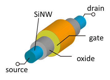
Nanowire: Fabrication and applications
Graphene Device: Carbon nanotube transistor fabrication, CNT applications
Module 01 : Environment and Crystal Growth for VLSI Technology
Environment: Semiconductor technology trend, Clean rooms, Wafer cleaning
Semiconductor Substrate: Phase diagram and solid solubility, Crystal structure, Crystal defects, Czochralski growth, Bridgman growth of GaAs, Float Zone growth, Wafer Preparation and specifications
Module 02 : Fabrication Processes Part 1
Deposition: Evaporation, Sputtering and Chemical Vapor Deposition
Epitaxy: Molecular Beam Epitaxy, Vapor Phase Epitaxy, Liquid Phase Epitaxy, Evaluation of epitaxial layers
Silicon Oxidation: Thermal oxidation process, Kinetics of growth, Properties of Silicon Dioxide, Oxide Quality, high κ and low κ dielectrics
Diffusion: Nature of diffusion, Diffusion in a concentration gradient, diffusion equation, impurity behavior, diffusion systems, problems in diffusion, evaluation of diffused layers
Ion Implantation: Penetration range, ion implantation systems, process considerations, implantation damage and annealing
Module 03 : Fabrication Processes Part 2
Etching: Wet chemical etching, dry physical etching, dry chemical etching, reactive ion etching, ion beam techniques
Lithography: Photoreactive materials, Pattern generation and mask making, pattern transfer, Electron beam, Ion beam and X-ray lithography
Device Isolation, Contacts and Metallization: Junction and oxide isolation, LOCOS, trench isolation, Schottky contacts, Ohmic contacts, Metallization and Packaging
CMOS Process Flow: N well, P-well and Twin tub
Design rules, Layout of MOS based circuits (gates and combinational logic), Buried and Butting Contact
Module 04 : Measurements, Packaging and Testing
Semiconductor Measurements: Conductivity type, Resistivity, Hall Effect Measurements, Drift Mobility, Minority Carrier Lifetime and diffusion length
Packaging: Integrated circuit packages, Electronics package reliability
Testing: Technology trends affecting testing, VLSI testing process and test equipment, test economics and product quality
Module 05 : SOI, GaAs and Bipolar Technologies
SOI Technology: SOI fabrication using SIMOX, Bonded SOI and Smart Cut, PD SOI and FD SOI Device structure and their features
GaAs Technologies: MESFET Technology, Digital Technologies, MMIC technologies, MODFET and Optoelectronic Devices
Silicon Bipolar Technologies: Second order effects in bipolar transistor, Performance of BJT, Bipolar processes and BiCMOS
Module 06 : Novel Devices
Multigate Device: Various multigate device configurations (device structure and important features)
Nanowire: Fabrication and applications
Graphene Device: Carbon nanotube transistor fabrication, CNT applications
ICT lec 01 dated 14-07-2017 contents : reference taken from
1. Solid State Devices Video by Prof. S. Karmalkar,IIT Madras ( lec 01 )
1. VLSI Technology Video by Dr. Nandita Dasgupta, IIT Madras (lec 01 )
1. Solid State Devices Video by Prof. S. Karmalkar,IIT Madras ( lec 01 )
1. VLSI Technology Video by Dr. Nandita Dasgupta, IIT Madras (lec 01 )
ICT lec 01 dated 14-07-2017 Videos
Video 1 : Semicondutor Technology : Fab lab at TSMC
Video 2 : Fab 32 - Intel's first high-volume 45nm chip factory
Video 3 : GLOBAL FOUNDRIES Sand to Silicon
Video 4 : Mark Bohr gets Small
| sand-to-silicon_32nm-version.pdf |
Refer for more more information on http://newsroom.intel.com/docs/DOC-2476#
ICT lec 02 dated 15-07-2017 handouts:
| semiconductor_clean_room__intro.pdf |
| semiconductor_manufacturing.pdf |
ICT lec 03 dated 20-07-2017 handouts:
| semiconductor_technology_trend.pdf |
ICT lec 04 to 06 handouts:
topic : IC packages
topic : IC packages
| ic_packages.pdf |
ICT lec 07 to 08 handouts:
Topic : Electronic packages reliability part A
Refer Chapter 15 from : Ebook of Glenn R Blackwell, " The electronic packaging", CRC press
failure_mechanisms.pdf : only for reference
NOTE : In failure_mechanisms.pdf, failure mechanims for semiconductor devices which is discussed in the pdf is NOT in ICT syllabus , but failure mechanisms related to electronics packages in the same pdf is within syllabus.
| reliability_concepts.pdf |
| electrical_failure_mechanisms.pdf |
| failure_mechanisms.pdf |
ICT lec 09 to 10 handouts
Topic : Electronic packages reliability part B
Refer Chapter 15 from : Ebook of Glenn R Blackwell, " The electronic packaging", CRC press
solder_joint_reliability.pdf : only for reference
Topic : Electronic packages reliability part B
Refer Chapter 15 from : Ebook of Glenn R Blackwell, " The electronic packaging", CRC press
solder_joint_reliability.pdf : only for reference
| solder_joint_reliability.pdf |
ICT lec 11 handout
Topic : Difference between Si and GaAs, MESFET Vs MOSFET
Topic : Difference between Si and GaAs, MESFET Vs MOSFET
| ict_mesfet_basics.pdf |
ICT lec 12 dated 31 -08-2017
Topic : MESFET structure, MESFET types E-mode MESFET and D-mode MESFET, working and characteristics
Topic : MESFET structure, MESFET types E-mode MESFET and D-mode MESFET, working and characteristics
| ict_mesfet_basics.pdf |
ICT lec 13 dated 01-09-2017 :
Topic : MESFET technology, Processing steps for Mesa-isolated MESFET, Digital Technologies:
a) BFT b) SDFT and c) DCFT
DCFT fabrication, Process flow for an etched-channel E/D technology, necessity of self-aligned gate, SAINT and T gate self aligned processes, Motivation for MMIC technology
Topic : MESFET technology, Processing steps for Mesa-isolated MESFET, Digital Technologies:
a) BFT b) SDFT and c) DCFT
DCFT fabrication, Process flow for an etched-channel E/D technology, necessity of self-aligned gate, SAINT and T gate self aligned processes, Motivation for MMIC technology
| ict_gaas_technology.pdf |
Following 3 documents (pdfs 1. mesa_isolation.pdf 2. mocvd.pdf 3. mbe.pdf) are supporting handouts : ONLY for reading and for Curious minds
| mesa_isolation.pdf |
| mocvd.pdf |
| mbe.pdf |
MID TERM 01 Syllabus from my part : updated 01-09-2017
Environment: Semiconductor technology trend, Clean rooms, Wafer cleaning
Packaging: Integrated circuit packages, Electronics package reliability
MID TERM 01 Related slides : also available in blackboard
| semiconductor_manufacturing_clean_rooms_rca_cleaning.pdf |
| ic_packages_final.pdf |
Refer Chapter 15 from ebook link given below :
https://drive.google.com/file/d/0B9sm0DlpF8i0ams5aDZQb2JQc3c/view?usp=sharing
| microsystems_failures_and_failure_mechanisms.pdf |
| electrical_failure_mechanisms.pdf |
| materialscreep.pdf |
| reliability_concepts.pdf |
ICT MIDTERM Test 01 dated 08-09-2017
| ict_mid_term_1_2017.pdf |
ICT lec 14 and 15 dated 14-09-2017 and 15-09-2017 :
Topic : Motivation for MMIC and MMIC technology
| ict_gaas_technology_mmic.pdf |
Following ppt mmic.pptx : ONLY for reading and for Curious minds
| mmic.pptx |
ICT lec 16 dated 21-09-2017
Topic : MODFET basics, MODFET fabrication, Optoelectronics devices : LED basics , Heterojunction LED and fabrication, Heterojunction Laser fabrication
Topic : MODFET basics, MODFET fabrication, Optoelectronics devices : LED basics , Heterojunction LED and fabrication, Heterojunction Laser fabrication
| modfet_technology_and_optoelectronics_device.pdf |
ICT lec 17 and 18 dated 22-09-2017 and 28-09-2017
Topic : SOI Technology
Topic : SOI Technology
| ict_soi.pdf |
ICT lec 19 and 20 dated 05-10-2017
Topic : Test Economics and product quality
Refer Chapter 3 from Ebook of Bushnell, " Essentials of Electronic Testing for digital, memory and mixed signal VLSI circuits, Springer
Topic : Test Economics and product quality
Refer Chapter 3 from Ebook of Bushnell, " Essentials of Electronic Testing for digital, memory and mixed signal VLSI circuits, Springer
| test_economics_and_product_quality.pdf |
ICT lec 21 dated 06-10-2017
Topic : Technology trends affecting testing, VLSI testing process and test equipment
Refer Chapter 3 from Ebook of Bushnell, " Essentials of Electronic Testing for digital, memory and mixed signal VLSI circuits, Springer
ICT lec 22 dated 12 -10-2017
Topic: Semiconductor measurement : Hot probe method for determining Conductivity type, Four- Probe method for resistivity measurement.
Refer: Semiconductor measurements Chapter 20 from M.S Tyagi , "Introduction to semiconductor materials and Devices".
Topic: Semiconductor measurement : Hot probe method for determining Conductivity type, Four- Probe method for resistivity measurement.
Refer: Semiconductor measurements Chapter 20 from M.S Tyagi , "Introduction to semiconductor materials and Devices".
ICT lec 23 dated 13 -10-2017
Topic: Semiconductor measurement : Van der Pauw method for resistivity measurement for odd shaped semiconductors, Haynes Shockley Experiment for measurement of i) Drift mobility ii) Diffusion co-efficient and minority carrier lifetime.
Refer: Semiconductor measurements Chapter 20 from M.S Tyagi , "Introduction to semiconductor materials and Devices".
Sample Mid term papers of 2016 and 2015
| ict_mid_term_1_2016.pdf |
| ict_re_mid_term_1_2016.pdf |
| ict_mt2_syllabus_2016.pdf |
| ict_paper_mt2__oct_2015.pdf |
List of Questions from other modules:
| list_of_questions.pdf |
University question papers
ICT Mam's part syllabus handouts
| cmos_design_rules___layout.pdf |
| nmos_design_rules___layout.pdf |
| cmos_inverter_fabrication_process_flow.pdf |
| crystal_growth_techniques___crystal_defects.pdf |
ICT Assignment 02
| ict_assng_02_2017.pdf |
ICT Experiment write-ups
| expt_01_cmos_inverter.pdf |
| expt_02_cmos_nand_nor.pdf |
| expt_03_sram.pdf |
| expt_04_expression.pdf |
| expt_05_tg.pdf |
Expt no. 06 : Study of IC packages
| ict_expt07_diffusion.pdf |
| ict_expt08_oxidation.pdf |
| ict_expt09_bulksingle_double_gate__mosfet.pdf |
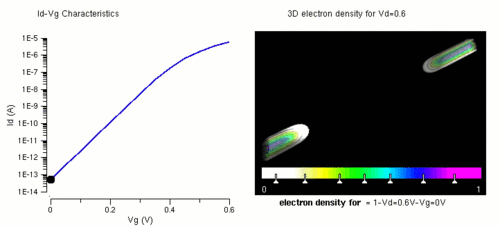
| ict_expt10_si_nanowire.pdf |
Last expt docs
| high_performance_silicon_nanowire.pdf |
| si_nanowire.pdf |
| simulations_of_carbon_nanotube_field_effect_transistors.pdf |
| multigate_mosfets.pdf |
| dgmosfets.pdf |
Expt no. 11 : Report on special topic
