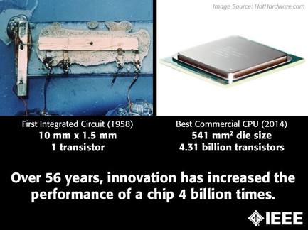
In 1958, Jack Kilby demonstrated the first integrated circuit (this is considered an IEEE milestone). Since then, microchip performance has followed the observations of Moore’s law. What that means is today’s chips are 4.3 billion times more powerful than Kilby’s first revolutionary circuit.
AVLSI Timing CLassification unit ppts
| avlsitiming_classification_of_digital_systems.pdf |
BVLSI Experiements
| bvlsi_01.pdf |
| bvlsi_02.pdf |
| bvlsi_03.pdf |
| bvlsi_04.pdf |
| bvlsi_05.pdf |
| bvlsi_06.pdf |
| bvlsi_07_mux.pdf |
| bvlsi_08.pdf |
| bvlsi_09_full_adder_4.pdf |
| bvlsi_10.pdf |
AVLSI Experiment
| avls_expt_7.docx |
AVLSI PDFs
| avlsitiming_classification_of_digital_systems.pdf |
| adv_vlsi_memory_rom.pdf |
| avlsi_arithmetic_ckts.pdf |
ANNOUNCEMENT
Please refer energy band diagram of MOS device under accumulation , inversion and depletion and MOSFET Capacitance topics strickly from CMOS Digital Integrated Circuits - Analysis and design by Sung Mo Kang
Please refer energy band diagram of MOS device under accumulation , inversion and depletion and MOSFET Capacitance topics strickly from CMOS Digital Integrated Circuits - Analysis and design by Sung Mo Kang
Energy band diagram of MOS device :Accumulation , inversion and depletion ( Latest)
| energy_band_diagram.pdf |
Inverter Switching Characteristics ( Latest )
Note : this topic was not covered in class
Note : this topic was not covered in class
| inverter_switching_characteristics.pdf |
POWER DISSIPATION IN CMOS CIRCUITS (LATEST)
Q . TYPES OF POWER DISSIPATION
Q. POWER DISSIPATION REDUCTION METHODS
Please Note : Read power dissipation pdf , before referring Sources of power dissipation
Q . TYPES OF POWER DISSIPATION
Q. POWER DISSIPATION REDUCTION METHODS
Please Note : Read power dissipation pdf , before referring Sources of power dissipation
| power__dissipation_in_cmos_circuits.pdf |
SOURCES OF POWER DISSIPATION IN CMOS CIRCUITS ( LATEST)
| sources_of_power_dissipation_in_digital_cmos_circuits.pdf |
Pass Transistor and Verilog ( Latest )
| pass_trans_verilog_vlsi_.pdf |
MOS CAPACITOR C-V Characteristics and Frequency effects ( Latest )
| mos_capacitor_cv.pdf |
SHORT CHANNEL EFFECTS ( LATEST)
| short_channel_effects_in_mosfets.pdf |
Class ppts of VLSI Module 3 (Semiconductor Manufacturing Process)
| module_iii_vlsi.pdf |
Syllabus for VLSI Mid Terms 2
1. Semiconductor manufacturing process Module ( Semiconductor manufacturing methods ( Mask Generation , Oxidation , CZ method , Photolithography , Ion implanatation , Diffusion and Metallization ) , Processing Steps for fabrication for Pmos , Nmos , Cmos p - Well , Cmos n-well , and Cmos twin tub process , CMOS LATCH -UP
2. Pass transistor and Transmission Gates ( 4:1 Mux , etc )
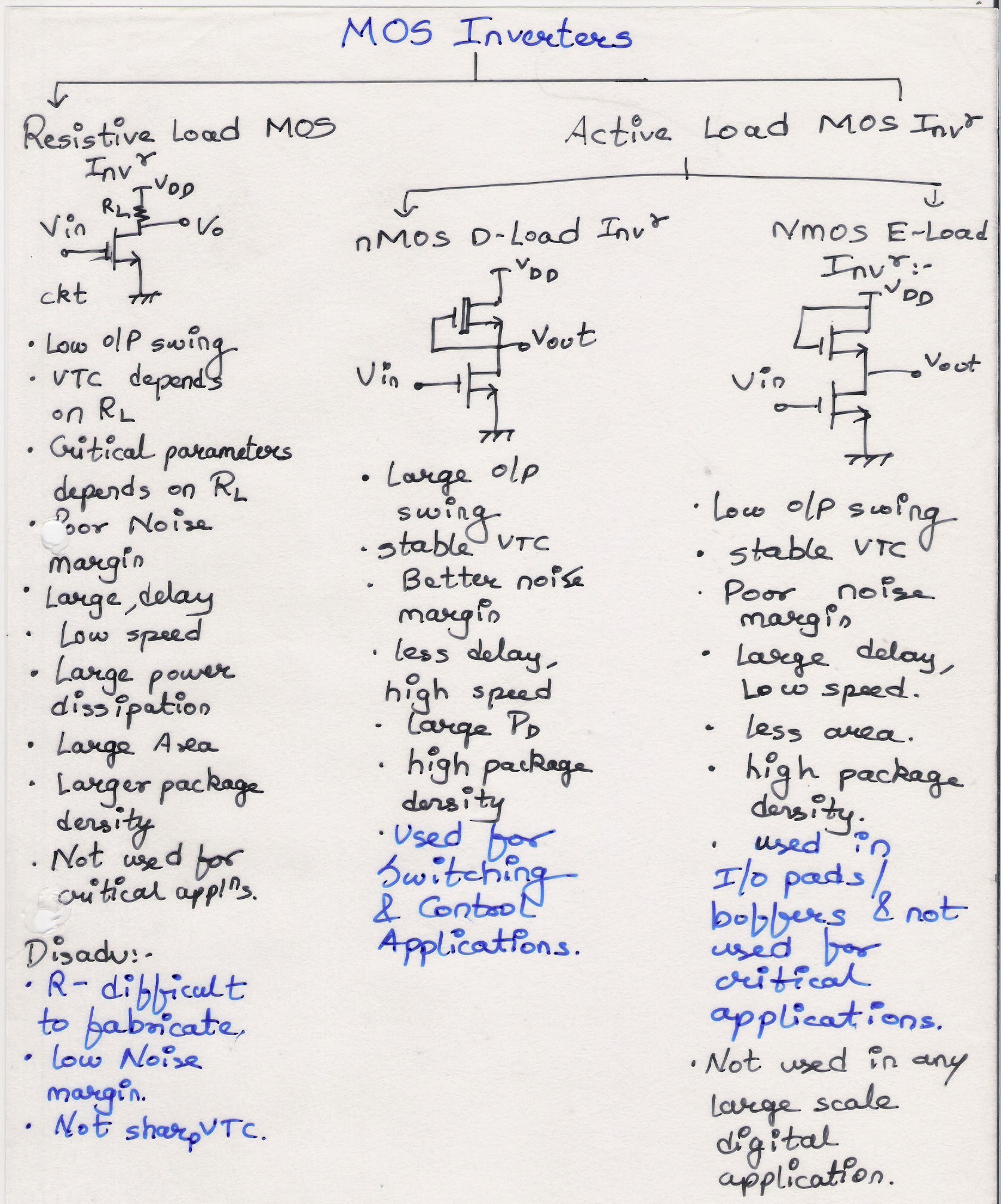
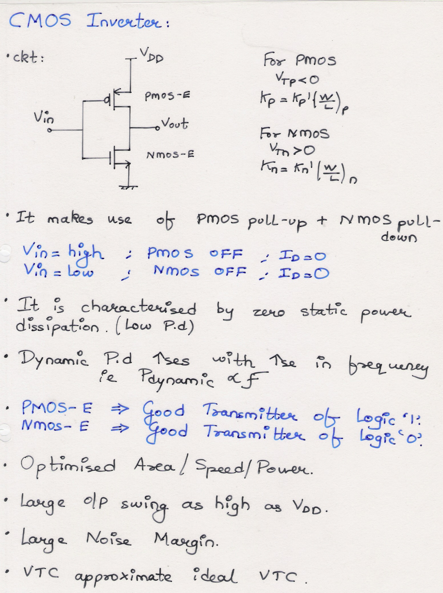
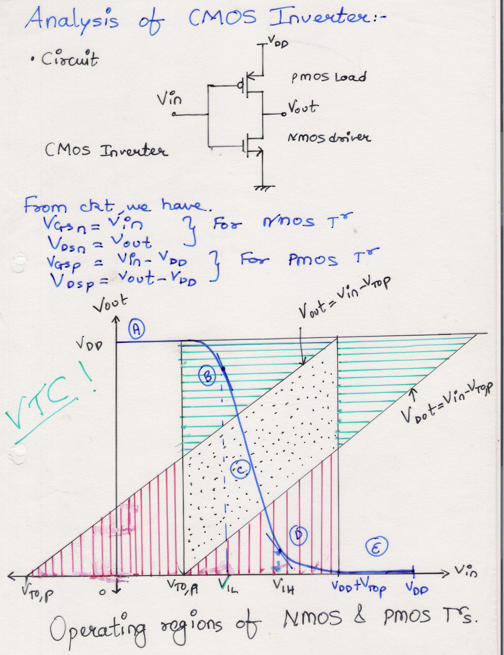
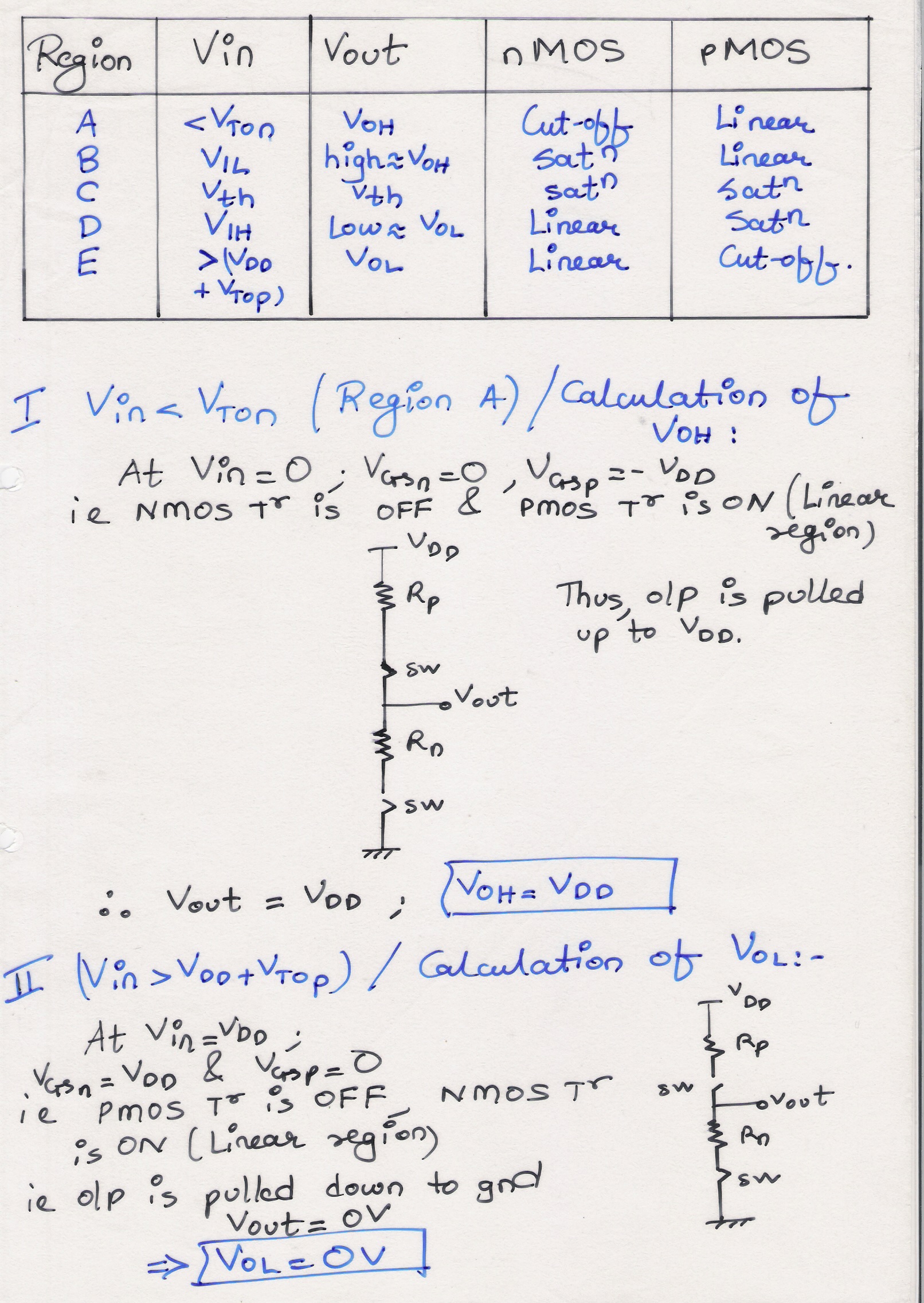
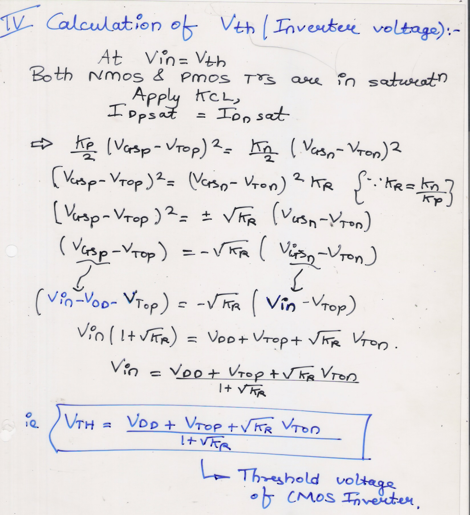
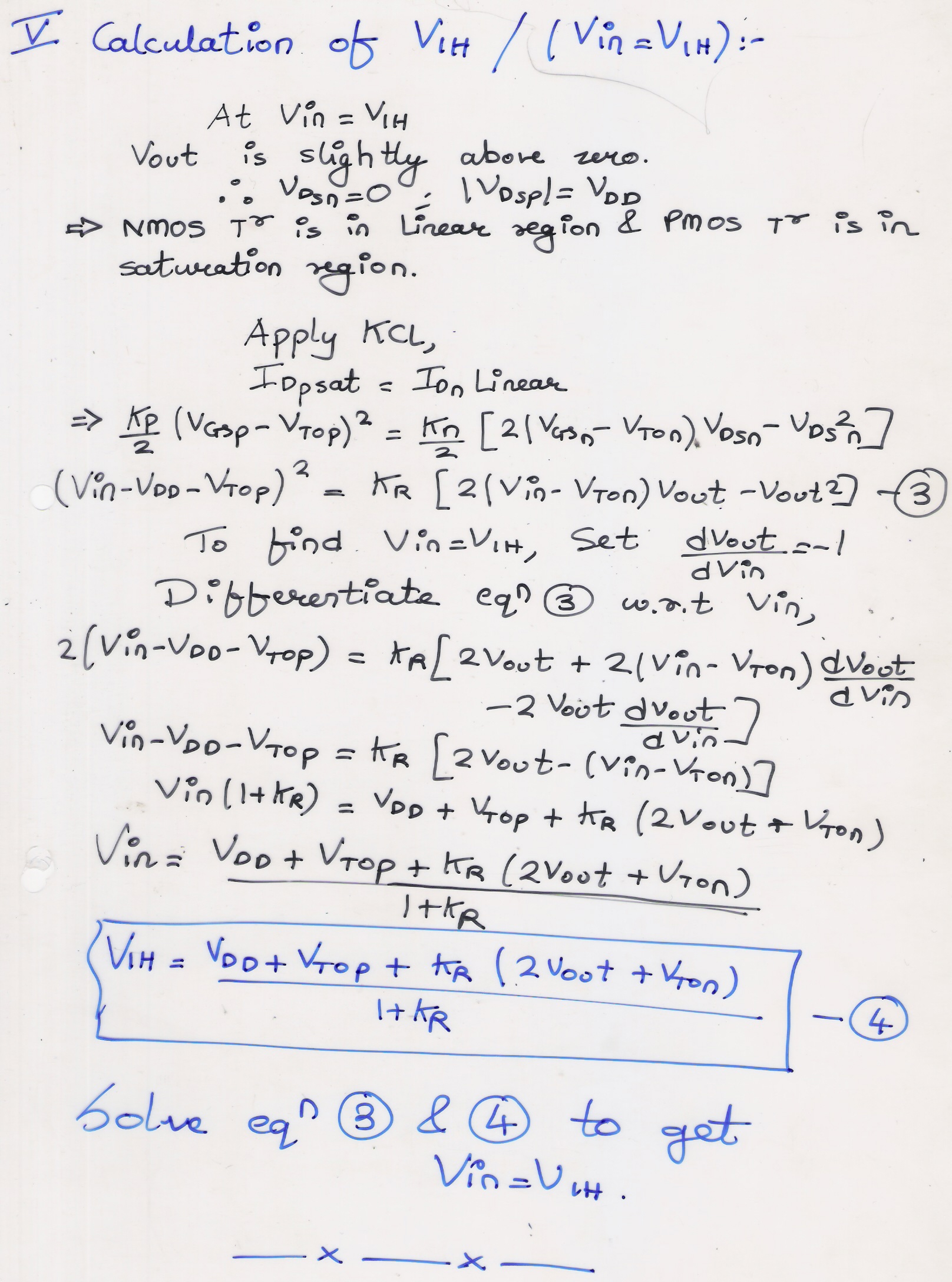
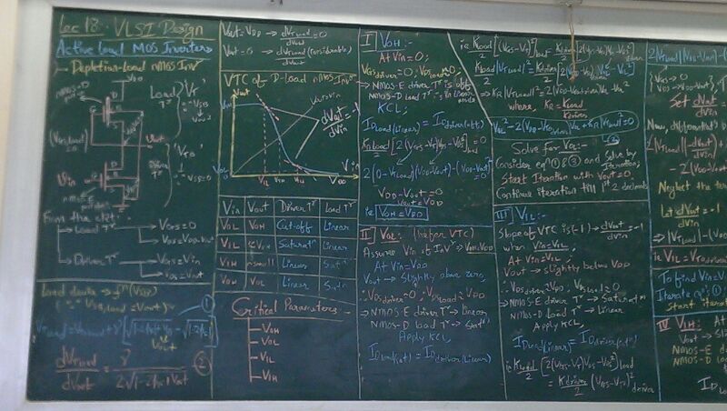
3. Mos inverter Module ( Concept of Noise Margin ( refer Univ Question and Kang ) , Resistive Load Nmos Inverter ( Derivation for Noise Margins + Numericals ) , Depletion load Mos Inverters ( Only Derivations ) , Inverter Sizing for one inverter driving another Inverter ( D-Load Nmos ) , CMOS Inverters ( Explanation and Derivation for 5 operation regions ) , Derivation for Switching or Threshold voltage for CMOS Inverters ( Plus Numericals) , Numericals on Noise Margins Calculation for a CMOS Inverter, VTC for CMOS Inverter inverter for different value of Kr.
1. Semiconductor manufacturing process Module ( Semiconductor manufacturing methods ( Mask Generation , Oxidation , CZ method , Photolithography , Ion implanatation , Diffusion and Metallization ) , Processing Steps for fabrication for Pmos , Nmos , Cmos p - Well , Cmos n-well , and Cmos twin tub process , CMOS LATCH -UP
2. Pass transistor and Transmission Gates ( 4:1 Mux , etc )
3. Mos inverter Module ( Concept of Noise Margin ( refer Univ Question and Kang ) , Resistive Load Nmos Inverter ( Derivation for Noise Margins + Numericals ) , Depletion load Mos Inverters ( Only Derivations ) , Inverter Sizing for one inverter driving another Inverter ( D-Load Nmos ) , CMOS Inverters ( Explanation and Derivation for 5 operation regions ) , Derivation for Switching or Threshold voltage for CMOS Inverters ( Plus Numericals) , Numericals on Noise Margins Calculation for a CMOS Inverter, VTC for CMOS Inverter inverter for different value of Kr.
Class ppts of VLSI Module 1
| vlsi_unit_1.pdf |
Class ppts of Design rules and Layout
| layouts_ds.pdf |
Semiconductor Simulation Applets
http://jas.eng.buffalo.edu/
http://jas.eng.buffalo.edu/
BE Electronics Syllabus
| be_7-8-etrx___syllabus.pdf |
SEM 7 University Question Papers
| june_2014_etrx.pdf |
| december_2013_all_subjects_etrx.pdf |
| december_2012_all_subjects_etrx.pdf |
| june_2012all_subjects_etrx.pdf |
| may_2011all_subjects_etrx.pdf |
| december_2011all_subjects_etrx.pdf |
| december_2010all_subjectsetrx.pdf |
How a Intel Processor is made : Amazing process
| intel_chip_design.pdf |
| from_sand_to_circuits.pdf |
Mosfet Transistor Basic
| 1.jpg |
| 2.jpg |
| 3.jpg |
| 4.jpg |
| 5.jpg |
| 6.jpg |
CMOS INVERTER Slides
| 1.jpg |
| 2.jpg |
| 3.jpg |
| 4.jpg |
| 5.jpg |
| 6.jpg |
| 7.jpg |
| 8.jpg |
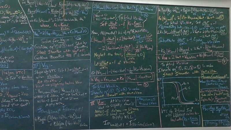
| board_33_vlsi.jpg |
| board_33_vlsi1.jpg |
CMOS Digital Integrated Circuits - Analysis and design by Sung Mo Kang Topic wise Slides
| chapter1_vlsi_basic_.pdf |
| physics_of_mos_transistor_.pdf |
| chapter5_mos_inverter_.pdf |
| chapter6_mos_inverter_dynamic_behaviour_.pdf |
| chapter7_nand_and_nor_design_.pdf |
Technical articles
| changing_the_transistor_channel.pdf |
| chipworks_reverse_engineering.pdf |
